
Graphene devices are showing amazing flexibility, and not just the mechanical kind. Researchers at Rice University and the University of California, Riverside, recently demonstrated an amplifier, based on a single graphene transistor, that can do the job of three different amplifiers. The device could lead to smaller, lower-power analog circuits, such as Bluetooth radios, they say. Separately, scientists at IBM are developing a type of graphene device that can be reconfigured, on the fly, into six different logic gates. Despite this, engineers agree that practical graphene logic is many years away.
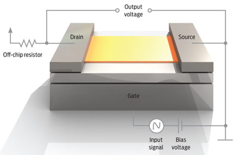
Graphene has many remarkable qualities, which its proponents say could make it a successor to silicon as a basis for electronics. One promising property is that it's ambipolar—both electrons and holes, positive charge carriers in semiconductors, can carry current through the material, and the application of voltage can control the contributions of the two types of carriers to the current through a device. This property enables a single graphene-based amplifier to act as more than one type of amplifier or potentially as a variety of logic gates.
"There's a growing consensus that people should consider ambipolarity a little more seriously," says Kartik Mohanram, an assistant professor of electrical engineering at Rice, in Houston.
Mohanram and his colleagues set about building the amplifiers using a single graphene transistor. In conventional complementary metal-oxide semiconductor (CMOS) circuits, the type of amplifier is determined by how it's built, and it can't be changed later. But thanks to ambipolarity, a graphene-based amplifier can switch types just by adjusting a voltage.
Depending on whether electrons or holes dominate the current, you get an n-type or a p-type field-effect transistor. The hole-rich p-type acts as a straightforward amplifier; the electron-rich n-type shifts the signal's phase by 180 degrees. If the flow of negative and positive carriers is equal, the transistor becomes a frequency multiplier. Switching signals in the device between two phases (phase-shift keying) or two frequencies (frequency-shift keying) allowed the team to encode digital data onto an RF signal.
Mohanram and his colleagues, aided by Alexander Balandin from the University of California, Riverside, published their proof-of-concept demonstration in ACS Nano in October.
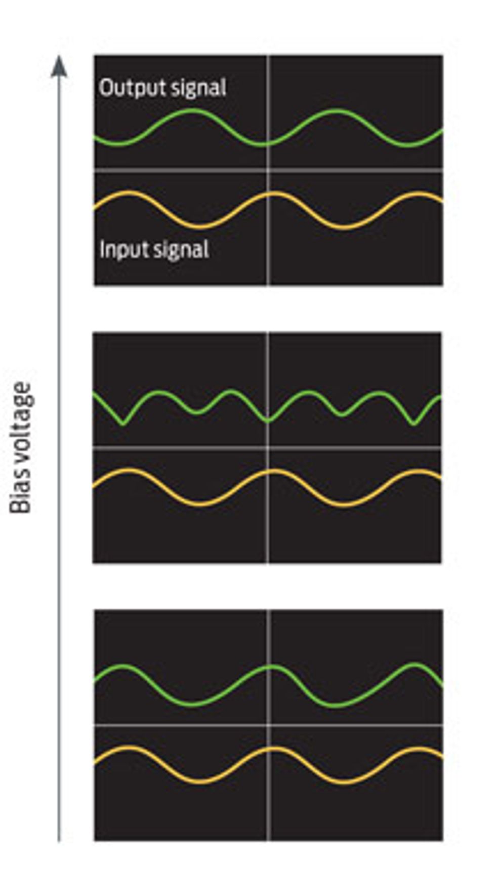
"What we were excited about was we could do phase-shift keying and frequency-shift keying with a single transistor," says Mohanram. A CMOS-based amplifier might require six transistors for the same functions, he says. Additionally, graphene circuits could handle much higher frequencies than their silicon counterparts. Engineers at IBM and the University of California, Los Angeles, have demonstrated graphene transistors with the potential for terahertz speeds. Silicon circuits, on the other hand, typically max out in the tens-of-gigahertz range.
IBM, too, is working on a graphene-based amplifier and radio-frequency transistor, part of a program funded by the Defense Advanced Research Projects Agency. Chun-Yung Sung, program manager for graphene nanoelectronics at IBM's Thomas J. Watson Research Center, in Yorktown Heights, N.Y., says he expects prototypes in about five years. The development of thin-film graphene could lead to flexible, printable circuits that can be reconfigured at will, Sung says.
While analog devices based on graphene may be just a few years in the future, the path to replacing silicon circuits with graphene-based logic remains a long one, says Mohanram.
That's because graphene naturally lacks a band gap, the property of semiconductors that controls the operation of transistors and other devices. One solution may be to sculpt the graphene into nanoribbons just a few nanometers wide, essentially squeezing the electric field within the material to produce a band gap [see "Graphene Electronics, Unzipped," IEEE Spectrum, November 2010].
Logic based on graphene will have to be built on a new concept, one that takes advantage of the material's unique properties, says Sung. Sung and his colleagues propose making a p-n junction out of sheets of graphene and applying positive or negative voltages to switch the electronic state of the material, providing an on-off switch. Depending on the voltages it is subject to, this device could switch between being a NOT gate, an OR gate, or an AND gate, among other functions.
"These revolutionary devices will come with revolutionary architecture," Sung says. And as CMOS shrinks closer to the point where it can't get any smaller—about 10 nanometers is expected—coming up with those architectures becomes more urgent. "We need to come up with device options before 2020," he says.