28 April 2010—With the advent of microelectromechanical systems (MEMS) and even tinier nanoelectromechanical systems (NEMS), the days of inserting a couple of AA batteries into a gadget and calling it a day are, at best, in technology’s side-view mirror. Supercapacitors hold a lot of promise as the successor to batteries, because they can be charged and discharged rapidly, don’t lose energy capacity when they’re recharged after incomplete discharges, and can stand up to an infinite number of charge-discharge cycles. Try as they might, though, engineers haven’t been able to design one whose energy storage capacity isn’t woefully meager compared to batteries.
But a team of researchers at Drexel University, in Philadelphia, report in the 23 April edition of Science that they have come up with a new microfabrication technique that will help engineers produce high-energy-density supercapacitors that can be built on a wafer right alongside the devices they power.
A supercapacitor typically is made from two porous electrodes soaked in an electrolyte solution with an insulator between them. When voltage is applied, ions from the electrolyte accumulate along the porous surfaces of two electrodes. The capacitance is greatly increased compared with that of ordinary capacitors, because pores give the electrodes an enormous surface area on which to collect charge.
Microsupercapacitors have been tried on chips before using carbon nanotubes, metal oxides, activated carbon, and various polymers as the electrodes, but they’ve all failed because of low capacitance, high impedance, and complex manufacturing protocols.
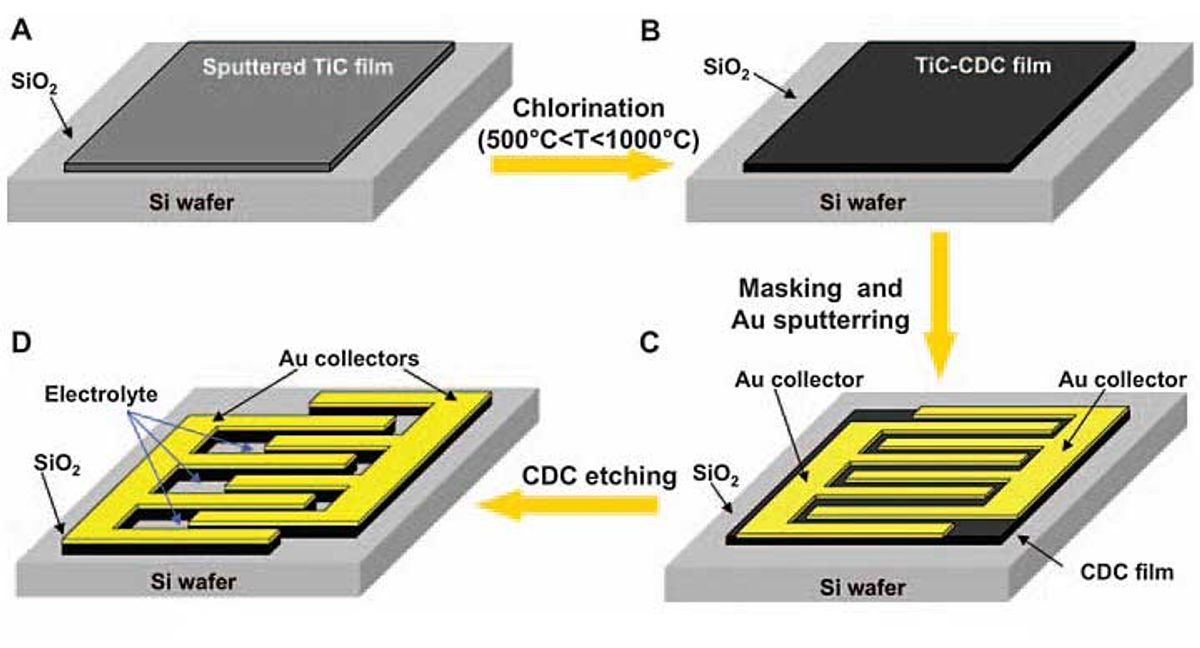
The Drexel team discovered that it could avoid these pitfalls by making the electrodes from titanium carbide–derived carbon. The chlorine-etching process they used to turn the carbide into carbon is very simple and is similar to the dry-etching techniques already used to make MEMS and microprocessors.
The process begins by depositing a 300-micrometer-thick layer of titanium carbide onto a silicon substrate using well-known chemical and physical vapor deposition techniques. The layer is exposed to 500 °C chlorine until a porous film of carbon builds up. The temperature setting is important, says Yury Gogotsi, a professor of materials science and engineering at Drexel who is a member of the research team. The aim is to remove metal atoms, he says, leaving pores that serve as storage bins for the electrolyte’s ions. Capacitance increases when pores are roughly equal to the size of the ions they are paired with. One problem with previous microcapacitor formulations is that these pores and their accompanying electrolytes were mismatched.
”At temperatures below 500 °C, the resulting pores are so small as to make the uptake of cations too slow or completely impossible,” says Gogotsi. That’s the chemical equivalent of sending a caravan of 3-meter-high trucks through an underpass with a 2.5-meter clearance. Temperatures higher than 500 °C result in pores that are too big. Space in the film’s volume is wasted, Gogotsi says, so fewer cations can be stored. Having pores much bigger than the cations also lowers the electric driving force, which diminishes the supercapacitor’s power density. Higher temperatures also cause the coating to build up so quickly that it’s difficult to control the thickness of the film. Thickness matters here, because capacitance drops off when the film exceeds a certain depth.
The Drexel researchers also found themselves able to adjust the pores’ arrangement within the film. They were able to eliminate gaps between pores, which they say resulted in a 40 percent increase in volumetric capacitance (measured in farads per cubic centimeter). Pore tuning—tweaking the pores’ size and surface chemistry—yielded another 50 percent improvement in capacitance over what was previously possible in chip-scale solid-state storage devices. Better still, says Gogotsi, control over these variables will allow manufacturers to design a device to maximize energy density or power density depending on the application.
Gogotsi says the group is testing the technology and hopes to have a prototype very soon. He says the technology has been licensed to Y-Carbon, a start-up based in King of Prussia, Pa., that will take it to the commercial stage.


