
Billions of chips in today’s computers, automobiles, cellphones, media cards, and those clever keychain memories are literally powerless when idle, yet they dispense data and instructions at the flick of the on-switch. They are almost all flash memory chips, a type of electrically erasable and programmable read-only memory.
Nonvolatility, flash’s property of retaining data for years when unpowered, is crucial for most electronic systems any more complicated than a light bulb. A flash chip in a computer tells it how to boot up. In a cellphone, it holds the instructions and data needed to send and receive calls, and stores phone numbers. Electronic products of all types, from microwave ovens to industrial machinery, store their operating instructions in flash memory.
Almost as important as flash’s nonvolatility is its programmability. It’s the feature that lets users add addresses, calendar entries, and memos to personal digital assistants and erase and reuse the media cards that store pictures taken with digital cameras.
But flash is under assault by technologies bent on proving they can do better. These upstart random access memories (RAMs) have little in common. The ferroelectric memory picks up on the electric fields inside certain atoms and the directions in which they point. The magnetoresistive type stores data as the either-or directions of the alignment of small magnetic regions in a ferromagnetic material. A third, Ovonic Unified Memory, is based on a material that switches between crystalline and amorphous phases.
Different as these technologies are, they share two advantages over flash. First, they can write data in a few tens of nanoseconds, like the dynamic RAMs in a computer’s main memory. Flash, on the other hand, takes at least a microsecond [see table].
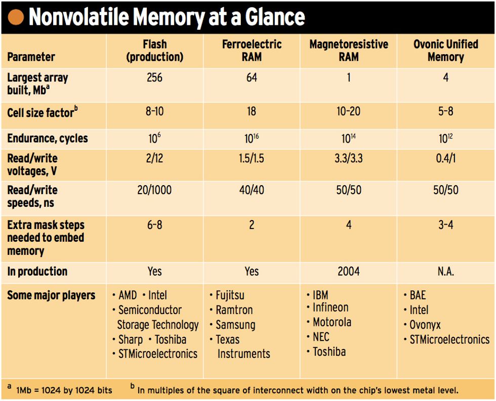
Second, the new memories can withstand constant rewriting for years, whereas flash cells begin to lose data after fewer than a million write cycles. Naturally, a million is fine for applications like media cards and cellphones, in which data may be written only a few times a day—as when a number is added to a cellphone’s address book or a picture is taken with a digital camera. But if used to constantly write new data, as in a computer’s main memory, flash cells would start breaking down in days or weeks. They also write much too slowly for computer-memory applications.
In contrast, the newcomers endure for a practically limitless number of write cycles. That endurance, together with their reasonable write speeds, takes them beyond flash to tackle the broader dynamic RAM market as well. DRAMs, after all, draw power continuously, even when data is not being read or written, and lose all data when power is switched off. Obviously, the electronics industry could be revolutionized by a memory as small as a DRAM and as fast, but able to retain data without drawing power.
A veritable pot of gold awaits such a successor to flash and DRAM. Taken together, flash and DRAM sales, which represent about 15 percent of the total semiconductor market, were projected last November by International Data Corp. (Framingham, Mass.) to total over US $22 billion in 2002 and exceed $25 billion in 2003. The big unanswered question is which one—or ones—will succeed?
Written in a flash
Flash technology works by storing electrons on a thin layer of polysilicon “afloat” in oxide below a transistor’s on-off control gate [see illustration, "Flash Relies on a Floating Gate"]. Called a floating gate, the scrap of polysilicon is electrically isolated by the surrounding oxide from the control gate above and the transistor’s channel below. (The channel is the short stretch of the transistor through which charge carriers flow when the transistor is on.) Apply a voltage to the control gate, and if there are no electrons on the floating gate, the device turns on; that could represent a 1. But if there is charge on the floating gate, the device does not turn on, and that could represent a 0.
Flash Relies on a Floating Gate
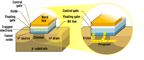 In a flash memory, the memory cell (left) is a CMOS transistor modified by the addition of a floating polysilicon gate and the tunnel oxide below it.
To write into the cell, electrons are blasted through the tunnel oxide from the channel and trapped on the gate. To erase data, electrons are forced to depart, often by tunneling through the same oxide. To read the cell, the word and bit lines are turned on, and the current in the bit line is measured. If excess electrons are on the floating gate, the current in the bit line is low; if there are none, it is high.Illustration: Steve Stankiewicz
In a flash memory, the memory cell (left) is a CMOS transistor modified by the addition of a floating polysilicon gate and the tunnel oxide below it.
To write into the cell, electrons are blasted through the tunnel oxide from the channel and trapped on the gate. To erase data, electrons are forced to depart, often by tunneling through the same oxide. To read the cell, the word and bit lines are turned on, and the current in the bit line is measured. If excess electrons are on the floating gate, the current in the bit line is low; if there are none, it is high.Illustration: Steve Stankiewicz
Reading a flash cell is simple—a matter of measuring whether or not voltage applied to the control gate turns the transistor on. But writing is a more complicated, two-step process.
First, charge is removed from the floating gates of a block of memory cells. Individual blocks can consist of several thousand transistors. Second, the cell is programmed by adding (or not adding) electrons to the floating gate. Many flash technologies program the cell by giving electrons enough energy to blast through the oxide below the floating gate, a process called hot-carrier injection.
This last operation affects charge retention. Electrons shooting through the oxide create defects that let charge leak between the floating gate and the channel. A separate voltage supply of up to 12 V is needed to give the carriers enough energy to plunge through the oxide, and that consumes power and complicates the design.
Enter the electric dipole
Already for sale, ferroelectric RAM products (FRAMs) are the most advanced of the flash challengers. The pioneer, Ramtron International Corp. (Colorado Springs, Colo.), has been selling FRAM chips since 1992. Their memory capacities are low, however, the largest being 256Kb—still a small fraction of the multimegabit chips offered by the major flash memory makers. In current commercial FRAMs, the interconnects that link individual transistors into circuits are 0.5 µm wide and operate at 3 V. Narrower interconnects are desirable so that memory cells may be made smaller and be packed in greater numbers onto an IC. (Ramtron’s FRAMs are made by Fujitsu Ltd., Tokyo, which also sells its own FRAM products, mostly as embedded memory in microcontrollers and smart cards.)
Ferroelectric Domains Do the Trick for FRAMs
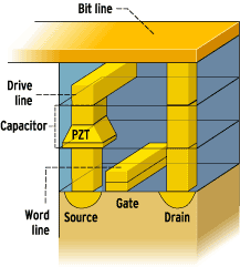 A ferroelectric RAM cell relies on a capacitor containing a lead-zirconium-titanate (PZT) insulator. Data is a 1 or a 0, depending on whether the ferroelectric domains in the PZT point up or down.
To program the cell, an electric field pointing up or down between the capacitor plates orients the domains up or down.
To read the cell, the bit and word lines are turned on and a short voltage pulse is applied to the capacitor through the drive line, creating an electric field. If the domains point in the same direction as the field, a small current pulse appears on the bit line. If they point in the opposite direction, a large current pulse occurs as the domains flip. Data is a 1 or 0, depending on whether the bit-line pulse is large or small.Illustration: Steve Stankiewicz
A ferroelectric RAM cell relies on a capacitor containing a lead-zirconium-titanate (PZT) insulator. Data is a 1 or a 0, depending on whether the ferroelectric domains in the PZT point up or down.
To program the cell, an electric field pointing up or down between the capacitor plates orients the domains up or down.
To read the cell, the bit and word lines are turned on and a short voltage pulse is applied to the capacitor through the drive line, creating an electric field. If the domains point in the same direction as the field, a small current pulse appears on the bit line. If they point in the opposite direction, a large current pulse occurs as the domains flip. Data is a 1 or 0, depending on whether the bit-line pulse is large or small.Illustration: Steve Stankiewicz
The biggest hurdle for FRAM developers is to advance the manufacturing technology to smaller geometries and lower voltages. R&D at Ramtron is aiming at 0.35-µm interconnect widths and 1.8-V operation. And last November, Texas Instruments Inc. (Dallas) announced that it had built a 64Mb FRAM in a standard 0.13-µm CMOS process, using technology licensed from Ramtron.
At the core of an FRAM cell is a capacitor filled with a ferroelectric crystalline material, usually a lead-zirconium-titanate (PZT) compound [see figure]. Each unit cell (a crystal’s basic building block) of a ferroelectric material has a permanent electric field around it. That’s because the geometric center of all the electrons in the unit cell is at a different spot from the geometric center of all the protons. It’s as though two small particles with equal and opposite charges are separated from each other by a short distance—in short, it is an electric dipole.
Many materials form electric dipoles. But what sets ferroelectric materials apart from other dipolar materials is that millions of dipoles, in a region called a domain, line up to point in the same direction. When an electric field is applied in the opposite direction, the dipoles flip over so that they again point in the direction of the electric field.
Each unit cell of PZT is shaped like an elongated cube. At each of the cube’s eight corners is an atom of lead; in the center of each cube face is an oxygen atom; and in the interior of the cube is an atom of either zirconium or titanium. This last has two stable positions, explains Mike Alwais, Ramtron’s vice president of FRAM products: “One is near the cube’s top face and the other is near the bottom.”
Apply an electric field and the atoms in the interiors of all the unit cells in the ferroelectric material move in the field’s direction. Remove the field and the atoms stay put. The positions of the atoms in the cubes store the bit of data, a binary 1 or 0.
To read a bit, an electric field is applied. If the atoms are near the cube “floors” and the electric field pushes them to the top, the cell gives off a current pulse. This pulse, representing a stored 1 or 0, is detected by a sense amplifier. Contributing to pulse amplitude are the movements of the interior atoms in the crystals of the ferroelectric material and the capacitor itself. If the atoms are already near their cubes’ “ceilings,” they don’t budge when the field is applied and the cell gives off a smaller pulse, due only to the electric charges stored on the cell capacitor.
Reading an FRAM cell destroys the data stored in its capacitor. So after the bit is read, the sense amplifier writes the data back into the cell, just as in a DRAM.
The FRAM in fact is like the DRAM in every way but one: the DRAM cell’s capacitor is of a nonferroelectric material, usually silicon dioxide. When data is stored as charge on the DRAM cell’s capacitor, the charge leaks away into the silicon substrate almost immediately—unless it is rewritten several times a second. That requirement drives up power consumption, and of course when the power is turned off, the charge stored in the capacitors quickly disappears.
Because the basic operation and structure of the FRAM and the DRAM are so similar, Alwais expects that FRAMs will eventually run as fast as DRAMs with the same memory capacity and cell size. Today, FRAMs are about 50 percent slower than DRAMs.
Texas Instruments is interested in FRAMs for embedded applications—for example, for on-chip storage of the operating instructions for digital signal processors and microcontrollers, says IEEE Fellow Dennis Buss, Texas Instruments’ vice president of R&D. Looking ahead, the biggest obstacle to embedding large memories on a chip is their high power consumption, particularly for wireless applications. “All our tricks to reduce the power used when the memory is idle [static power] are just not adequate for battery-operated systems,” says Buss. “That’s why we are looking at integrated memory technologies that reduce the static power to zero.”
Each of the three new memory technologies—ferroelectric, ferromagnetic, and Ovonic—has zero static power. Texas Instruments has studied the merits of all of them, but has chosen to develop FRAM. One reason for the choice is economic, according to Buss. The desired patterns of semiconductors, insulators, and metals are “stenciled” onto the chips through masks, which are quartz plates covered with chrome stencils. Today’s IC chips usually need a succession of 20 to 26 masks, and the more masks, the more complicated and expensive the manufacturing process.
Ferroelectric memory needs only two extra masks added to a chip’s manufacturing process, says Buss. So it is much less expensive than magnetic memory, which requires four extra masks. FRAM’s maturity is also in its favor. “Fujitsu and Ramtron have shipped more than 100 million chips with up to 256Kb of FRAM,” Buss adds. “What we want to do is take it to much higher densities.”
MRAMs Do It With Tiny Magnets
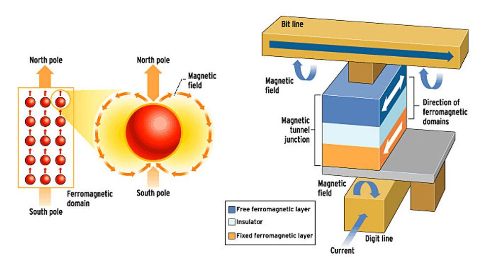
Magnetoresistive RAMs (MRAMs) exploit ferromagnetism to store data. Each atom in a ferromagnetic material is a tiny magnet with a north and a south pole [above]. Atoms lined up with their north poles pointing in the same direction form ferromagnetic domains.
In one type of MRAM cell [right], two layers of ferromagnetic material separated by a thin insulation layer form a magnetic tunnel junction. The direction of the domains in the bottom layer is fixed, while those in the top layer can switch when a magnetic field is applied. Whether a 1 or 0 is stored depends on whether the two layers’ magnetic domains point in the same or opposite directions.
Reading the cell involves measuring the resistance of the tunnel junction. It is low if the domains in the two layers are parallel, high if they are antiparallel.
Writing data into the cell involves applying current to the bit and digit lines. The magnetic fields created by the two currents line up the magnetic domains in the desired direction. In the case here, current from left to right in the bit line and into the page in the digit line align the free ferromagnetic layer in the same direction as the fixed layer.
At present, Texas Instruments uses flash to fill its nonvolatile memory requirements. Because it would take six to eight extra masks to embed flash with other circuits on the same chip, says Buss, the company finds it cheaper to buy a flash chip, stack it on top of a digital signal-processor chip, and package the two together. “But because FRAM needs only two additional masks, we will be able to build it on the same chip,” Buss continues. He expects that embedded FRAM products from his company could be in production by 2005.
MRAM: Spinning a new memory
The second new memory technology turns to another property of some atoms, ferromagnetism. All atoms in a ferromagnetic material act like tiny magnets and respond to an external magnetic field by trying to align themselves in its direction. As in ferroelectric materials, they arrange themselves into domains in which all the atomic magnets point in the same direction, creating a larger magnet [see figure].
Apply an external magnetic field and all of the domains line up to point in its direction; remove the field and they remain locked in that direction. If a field is next applied in the opposite direction, the domains flip over.
This property—that the magnetic domains of ferromagnetic materials change direction only when they are influenced by a magnetic field—makes them ideal memory devices. They have been used as magnetic memory almost from the first days of computers, first in the iron toroids of core memory, then later in hard drives. Now, ferromagnetic materials are being used in semiconductor magnetoresistive RAMs, or MRAMs.
At the IEEE’s Symposium on VLSI Circuits held in June of last year in Honolulu, Hawaii, Motorola researchers announced the largest MRAM to date—1Mb. The company has been developing the technology since 1995 and expects to have MRAMs in production in 2004, with samples available this year.
Of several approaches to making the magnetoresistive devices, Motorola researchers have chosen the magnetic tunnel junction as the basis of its memory cell. These junctions are composed of two ferromagnetic layers separated by a thin layer of insulator. At thicknesses of more than a few nanometers, the insulator bars the passage of electrons. But in tunnel junctions, the oxide is less than 2 nm thick so that some electrons can tunnel across it from one ferromagnetic layer to the other.
In one of the magnetic layers, the domains are fixed in one direction. In the other, they reverse direction in response to an external applied magnetic field. As a result, they can be either parallel or antiparallel to the fixed layer. These two conditions store the 1s and 0s of the data.
Reading is straightforward. A transistor in the memory cell, which isolates the tunnel junction from the rest of the array when it is turned off, is turned on and the junction’s resistance is measured. If the two magnetic layers are parallel, the resistance is low; if they are antiparallel, it is high. What determines whether the resistance is high or low is whether it matches that of a reference cell. In Motorola’s 1Mb MRAM, one reference cell is needed for every 64 memory cells.
Data is written into the cell by passing a current through two wires: a bit line that runs over the magnetic tunnel junction, and a digit line that runs under it. The sum of these two currents creates a magnetic field strong enough to flip the domains in the free layer.
There are several key challenges to making MRAMs. One is the difficulty of integrating the fabrication of the magnetic tunnel junction into a CMOS fabrication line. Magnetic materials can mean sudden death to ICs if they contaminate the tools or materials used for the silicon transistors.
The way to counter that, says Saied Tehrani, MRAM technology director at Motorola Semiconductor Products Sector (Austin, Texas), is to track the batches of wafers after tunnel-junction fabrication and clean them thoroughly before bringing them into the CMOS line. “You have to have a good tracking system so you can evaluate where you have to do the cleaning and the measurements,” he says. Motorola builds the tunnel junctions near the end of the fabrication process, after the transistors have been built and most of the interconnect layers have been put down.
The second challenge involves the thin insulator at the center of each magnetic tunnel junction. It must be uniform across the wafer, because the resistance of a tunnel junction varies exponentially with insulator thickness. Tight process control is the answer, says Tehrani. Motorola has been able to produce 1.5-nm insulating layers that vary by only 1 percent across 200-mm wafers.
A third challenge is to ensure a large difference in the resistance between the parallel and antiparallel states of the memory cell. In 1995, when Motorola researchers began to develop MRAMs, the difference was only 5-6 percent. “Now we are talking about 40-50 percent,” says Tehrani, “[so we are] much more competitive with other memory technologies in the time it takes to read data from the cell.”
Besides Motorola, IBM Corp. has been developing MRAMs for seven years, and in 2000 began working with Infineon Technologies (Munich, Germany) to develop a commercial MRAM process. And last September, Toshiba and NEC teamed up to develop MRAMs.
But why bother with messy magnetic materials and ultrathin insulators? In a word, speed. MRAM could be faster than FRAM and even faster than DRAM, given comparable dimensions and capacities. Reading an MRAM cell, unlike reading a DRAM or FRAM cell, does not destroy data; so the time between successive memory operations can be shortened proportionally. And memory densities should be very high since an MRAM memory cell, like an FRAM or DRAM cell, has only one transistor.
OUM Heats Up, Then Cools Down
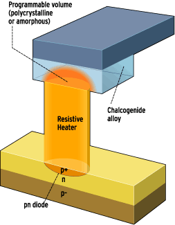 The Ovonic Unified Memory (OUM) is based on a chalcogenide alloy, which after being heated and cooled adopts one of two stable but programmable phases: polycrystalline or amorphous. Resistance of the first phase is low; of the second phase, high. A 1 or 0 depends on the phase of the programmable volume, determined by measuring its resistance.
To make the programmable volume amorphous, it is heated above its melting point by the resistive heater. It cools rapidly when the heater is turned off. To make it crystalline, it is heated to just below its melting point for 50 ns, so that the atoms line up in their crystalline locations.Illustration: Steve Stankiewicz
The Ovonic Unified Memory (OUM) is based on a chalcogenide alloy, which after being heated and cooled adopts one of two stable but programmable phases: polycrystalline or amorphous. Resistance of the first phase is low; of the second phase, high. A 1 or 0 depends on the phase of the programmable volume, determined by measuring its resistance.
To make the programmable volume amorphous, it is heated above its melting point by the resistive heater. It cools rapidly when the heater is turned off. To make it crystalline, it is heated to just below its melting point for 50 ns, so that the atoms line up in their crystalline locations.Illustration: Steve Stankiewicz
Memory under glass
Key to the Ovonic Unified Memory (OUM) is a material called a chalcogenide, which is any alloy containing sulfur or selenium or tellurium. Chalcogenides show up in optical fibers and rewriteable CDs and DVDs. The Ovonic device is an alloy of germanium, antimony, and tellurium. It is useful as a memory because it can switch rapidly, when heated and then cooled, between stable amorphous and crystalline phases. These phases store the data’s 1s and 0s.
In the amorphous phase, the material has low reflectivity and a high resistance. In the crystalline phase it is reflective and has a low resistance. This feature is applied in rewriteable CDs and DVDs.
A memory cell consists of a top electrode, a layer of the chalcogenide, and a resistive heating element [see figure]. The base of the heater is connected to a diode. As with the MRAM, reading the micrometer-sized cell is done by measuring its resistance. But unlike the MRAM, the resistance change is very large—more than a factor of 100.
To write data into the cell, the chalcogenide is heated past its melting point and then rapidly cooled to make it amorphous. To make it crystalline, it is heated to just below its melting point and held there for approximately 50 ns, giving the atoms time to position themselves in their crystal locations.
OUM may well be both the oldest and the newest nonvolatile technology. It was first proposed as a memory in the 1960s by its developer Stanford Ovshinsky, cofounder, president, and chief executive officer of Energy Conversion Devices Inc. (Rochester Hills, Mich.). But those early devices were slow, devoured power, and tended to degrade owing to the large currents needed to write and erase data. It was not successful commercially, says Steve Hudgens, chief technology officer and vice president of research at Ovonyx Inc. (Santa Clara, Calif.), the company developing the memory now.
The success of rewriteable optical disk storage was indirectly responsible for OUM’s second wind. “During the 1970s and 1980s,” explains Hudgens, “several companies got very interested in rewriteable optical disks and developed materials with very fast crystallization speeds, including the germanium-tellurium-antimony alloy that we are currently using.”
The new material benefited both optical and electronic memory because it requires much less time and energy to program a bit. “That made it practical to program the optical disk with a semiconductor diode laser and to program an OUM cell with a short current pulse, which is what we need to produce a commercially competitive nonvolatile memory,” says Hudgens.
One area of concern as designs move to smaller dimensions is how close memory cells can be to one another before programming one alters the state of a neighbor. “Fortunately,” says Tyler Lowrey, Ovonyx’ president and chief executive officer, “the amount of heat needed to write a bit of data will also get smaller as the cell size shrinks, so the thermal profile should look the same in every generation.”
The largest memory made to date (at least, the largest the company will talk about) is a 4Mb array built with partner Intel Corp. (Santa Clara, Calif.), which is championing the technology. Ovonyx is also partnering with two European semiconductor makers, STMicroelectronics NV (Geneva, Switzerland) and BAE Systems PLC (Farnborough, UK). To develop a new technology into a commercial product, “you’ve got to look at statistics for millions and millions of bits. You have to work with companies that know how to do that,” says Hudgens. (Both Intel and STMicroelectronics have thriving flash memory businesses.)
All three partners have OUM parts running in their CMOS fabrication facilities. STMicroelectronics wants to replace flash memory. BAE Systems finds OUM a godsend for space applications because it is impervious to cosmic radiation, which can cause errors in memories based on charge storage, like DRAM. As for Intel, it isn’t divulging its plans.
No sitting duck
It will be many years before the sun sets on flash memory, according to Bomy Chen, vice president of technology for Silicon Storage Technology Inc. (Sunnyvale, Calif.)
For one thing, a flash cell can store more than one bit. A 2-bit flash cell was pioneered in 1996 by SanDisk Corp. (also in Sunnyvale) and the 2-bit-per-cell StrataFlash in 1997 by Intel. Now many companies make flash products that store multiple bits per cell, says Chen. That makes flash very inexpensive. And cost is one of the most important factors when product developers select components.
An interesting variation on floating-gate memories, variously called Monos, Sonos, Mirrorflash, or NROM, depending on the company developing it, promises to improve on flash’s poor endurance. The idea is to replace the polysilicon floating gate with a layer of nitride. Nitride is an insulator, so electrons storing data in it do not move around. “Defects in the oxide surrounding the nitride may cause some local loss of [electrons] just in that region, but overall the nitride holds onto its charge,” explains Craig Swift, memory device technologist, at the Motorola Semiconductor Products Sector.
Another benefit of electrons being glued to one place is the ability to store two bits of data on the nitride: one bit on each end of the nitride gate. Similar technology is under development by Saifun Semiconductors Ltd. (Netanya, Israel) together with its partners AMD and Fujitsu.
Chip size is another factor. “Customers don’t want to grow their chip size by even 3 percent,” says Chen. “And OUM, FRAM, and MRAM are 200-400 percent bigger than flash.” Of course, flash’s competitors believe that their cell sizes will shrink as the technologies mature, until they match those of flash and DRAM.
Then, too, the new nonvolatile memories have not amassed the multitudes of statistics needed to prove reliability and performance in a commercial product. “Each technology takes many years and lots of effort to become production-worthy,” notes Chen.
This point has not been lost on the developers of the alternative memories. “Any new memory technology is very difficult to bring on-line,” says Ovonyx’ Lowrey. “We’ve got to be low cost and compatible with existing processes, and then we have to show that we can do it in a production environment consistently, day in and day out.”
To Probe Further
Nonvolatile Semiconductor Memory Technology, edited by William D. Brown and Joe E. Brewer (IEEE Press, 1998), offers detailed explanations of flash and Sonos operation.
More in-depth information on FRAM may be found on Ramtron International Corp.’s Web site at https://www.ramtron.com/aboutfram/technology.htm.
An article on the basics of MRAM operation is available on the IBM Research Web site at https://www.research.ibm.com/thinkresearch/pages/2001/20010202_mram.shtml.
For background on the Ovonic Unified Memory, go to the technology frame of Ovonyx Inc.’s Web site, https://www.ovonyx.com/ovonyxtech.html.