The Conversation (0)

Photo: Karlsruhe Institute of Technology/Applied Physics Letters
For a century or more, nearly all technological advances have depended on our ability to produce and manipulate the vast variety of materials that nature has given us. Nowhere is that dependence more evident than in the field of electronics. From a smorgasbord of semiconductors, polymers, and metals, we’ve been able to create a dazzling array of circuitry that now underpins pretty much every aspect of modern life.
So now imagine what we could do if we weren’t limited to the materials found in nature. Researchers have long believed that it would someday be possible to produce artificial materials, or “metamaterials,” and that they would bring about some stunning, otherworldly technologies—the sort that have figured in science fiction tales for years. These innovations include invisibility cloaks that could mask the presence of objects or their electromagnetic signatures, “unfeelability cloaks” that could mechanically mask the tactile feel of an object, superlenses that could resolve features too small to be seen with ordinary microscope lenses, and power absorbers that could capture essentially all of the sunlight hitting a solar cell.
To achieve these advances we’ll need better metamaterials, and those are on the way. Metamaterials are made up of “meta-atoms”—small two- or three-dimensional structures made of polymer, dielectric material, or metal. When these structures are arranged in regular, repeating crystals, they can be used to manipulate electromagnetic radiation in new ways. Ultimately, the capabilities of a metamaterial are determined by the size, shape, and quality of these structures. And the technology to fabricate meta-atoms has recently turned a corner.
Over the past few years, research groups around the world have succeeded in developing a way to draw meta-atoms using lasers. The resulting structures can now take on nearly any shape and be stacked in three dimensions in dense, crystal-like arrangements. What’s more, they can be made small enough to exhibit unique mechanical and thermal properties and to alter the flow of light in a range of wavelengths—including the long-inaccessible visible chunk of the spectrum. Thanks to this microscopic fabrication technology, we can finally see a path beyond the materials nature has provided us into entirely new realms that are limited only by our imaginations.
Writing Through Resist: Constructing minute 3-D structures on a microscope
As diverse as natural materials are, they actually have a fairly narrow range of properties. That fact becomes quite evident in the way materials respond to light.
Ordinary atoms, such as silicon and copper, are full of charged particles and typically interact quite strongly with electric fields. But an electromagnetic wave is made up of two pieces: an oscillating electric field and an oscillating magnetic field. And the response of materials to magnetic fields is another story.
For a few quantum mechanical reasons we won’t get into here, many atoms do respond to the magnetic component of electromagnetic radiation (this response is what enables, for example, magnetic resonance imaging). But most atoms stop resonating—and thus responding—to the magnetic component of light when incoming radiation has a frequency above about 100 gigahertz, the high-frequency edge of the microwave part of the spectrum. That means, effectively, that conventional materials respond only to the electric part of an electromagnetic wave, particularly at infrared and visible wavelengths.
That might have been the end of the story. But in 1999, physicist John Pendry of Imperial College London and colleagues pointed out that it should be possible to create transparent structures that can manipulate both the electric and magnetic components of light.
To do this, the group devised a metallic ring with a slit cut out in the side. Like any metal loop, this split ring will resist a change in an external magnetic field with an inductance, or L. But because the loop has a gap in it, it will also accumulate charge on each side of that gap, giving the ring a capacitance, or C. The result is an LC circuit. Given an incoming electromagnetic wave with the right frequency, the split ring will respond with an oscillating current, and thus an oscillating magnetic field, of its own. The smaller the ring, the shorter the wavelength it will respond to.
Pendry and his coauthors reasoned that by arranging many such artificial structures in a dense, periodic array—a two- or three-dimensional crystal—it should be possible to create metamaterials that respond to incoming electromagnetic radiation in a way that natural materials don’t. In 2000, about a year later, a team led by David Smith and Sheldon Schultz at the University of California, San Diego, performed the first experiment that really demonstrated what metamaterials can do.
Smith and Schultz built 6.5-millimeter-wide split-ring resonators made of copper and spaced them out every 8 mm or so, placing a short length of wire in between each pair of resonators. When the researchers shone microwave radiation on the resulting structure, they showed that the material exhibited a mind-boggling property that doesn’t exist in nature: a negative index of refraction.
A material with this property more or less puts light in reverse gear. The best way to see how this works is to consider two parameters that are used to describe light propagation—the velocity of electromagnetic energy propagation and the phase velocity. The first describes the overall flow of the light, and the second describes how the light waves—the individual peaks and troughs—move. In an ordinary material, electrons respond to incoming fields by jiggling in such a way that they create their own electromagnetic field. The resulting field—a combination of the incoming field and the material’s response—will move in the same direction as the incoming radiation does, albeit with some lag and at a lower speed. As with the incoming field, both the energy and phase vectors are positive. But in a material with a negative index of refraction, energy and phase move in opposite directions. Although the energy of the light—and the light itself—still moves in the same direction as when it entered the material, the individual peaks and troughs actually move backward.
To picture how this would look in the real world, imagine a straw resting inside a half-filled glass. If the straw is standing in water, it will appear much as it does in air, with only a slight kink at the interface between the two materials. But if the glass contained a liquid with a negative refractive index, the straw would look bent, as if it were leaning in the opposite direction.
A material with a negative index of refraction could potentially be used to make superlenses capable of imaging objects at resolutions far below the wavelength of light that’s shone on them. But the ability to control both components of light also offers other possibilities. Meta-atoms designed to act on both the electric and magnetic components of radiation equally, for example, could be used to create an “invisibility cloak” that works on the naked eye, steering light so that an object can be hidden from view.
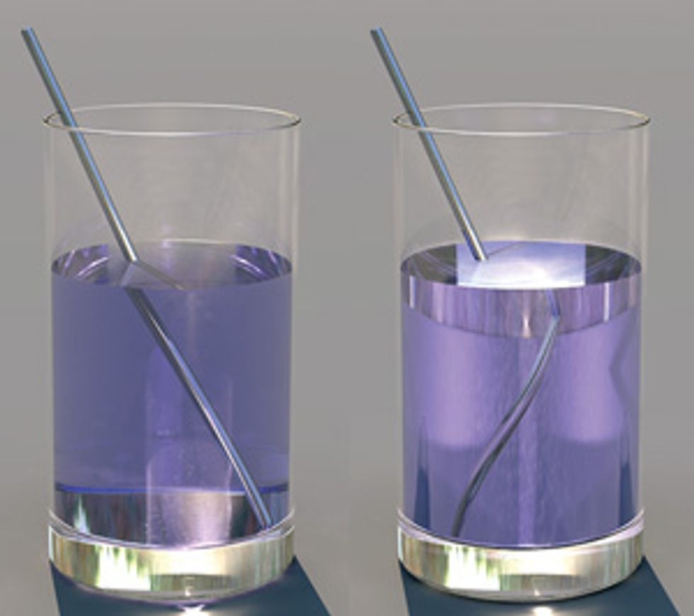 A Negative Bent: Artificial materials can be made to have a negative index of refraction, a light-bending property not seen in nature. The interface of air and water—two substances with positive indices—creates a small kink in the appearance of a straw (left). If the liquid had a negative index of refraction, the straw would appear to bend in the opposite direction (right).Photo: Karlsruhe Institute of Technology/Optics Express
We could also potentially make a metamaterial with electric and magnetic responses that destructively interfere, so that no radiation is reflected. If we could make that happen in a system that also absorbs light, we could create a perfectly black material that neither reflects nor transmits light, raising the possibility of more-sensitive detectors and more-efficient solar cells.
One other possible application is to filter out light with either a right- or left-handed circular polarization. The basic mechanism is similar to the way that sugar water, DNA, and other chiral materials—molecules with a physically distinct mirror image—rotate the polarization of a light wave. In those materials, the interaction is fairly weak, requiring light to travel for centimeters through the substance before it registers a strong change in polarization. A metamaterial, structured as an array of tiny helices, can accomplish its filtration task over much shorter distances. That could allow us to build compact devices that distinguish, for example, between pharmaceuticals and their mirror images, which may be identical in composition but have very different biological effects.
That’s only a small sampling of what might be done with metamaterials. To get from blueprint to reality, we have to find a good way to make the underlying structures—the meta-atoms.
When the metamaterials field got its start a bit more than a decade ago, meta-atoms tended to be macroscopic: centimeter-size metallic split rings and wires printed on standard circuit boards. But these structures were so large they could act only on longer-wavelength radiation, in the microwave part of the spectrum. To make metamaterials that can act on visible light, which has a wavelength range of roughly 400 to 750 nanometers, the “atoms” must be on the order of 100 to 200 nanometers or smaller.
How do you make such small structures? You might think that a natural place to start is with the technology that’s already been developed by the semiconductor industry. There are, after all, already powerful patterning tools, such as photolithography and electron-beam lithography, that are routinely used to fabricate submicrometer and nanoscale structures.
Indeed, groups such as those of Harald Giessen at the University of Stuttgart, in Germany; Vladimir Shalaev at Purdue University, in Indiana; Costas M. Soukoulis at Iowa State University; Xiang Zhang at the University of California, Berkeley; Nikolay Zheludev at the University of Southampton, in England; and ours at the Karlsruhe Institute of Technology (KIT), in Germany, have successfully used these techniques to create arrays of simple metamaterial structures, including split-ring resonators, that are small enough to act on visible or infrared light.
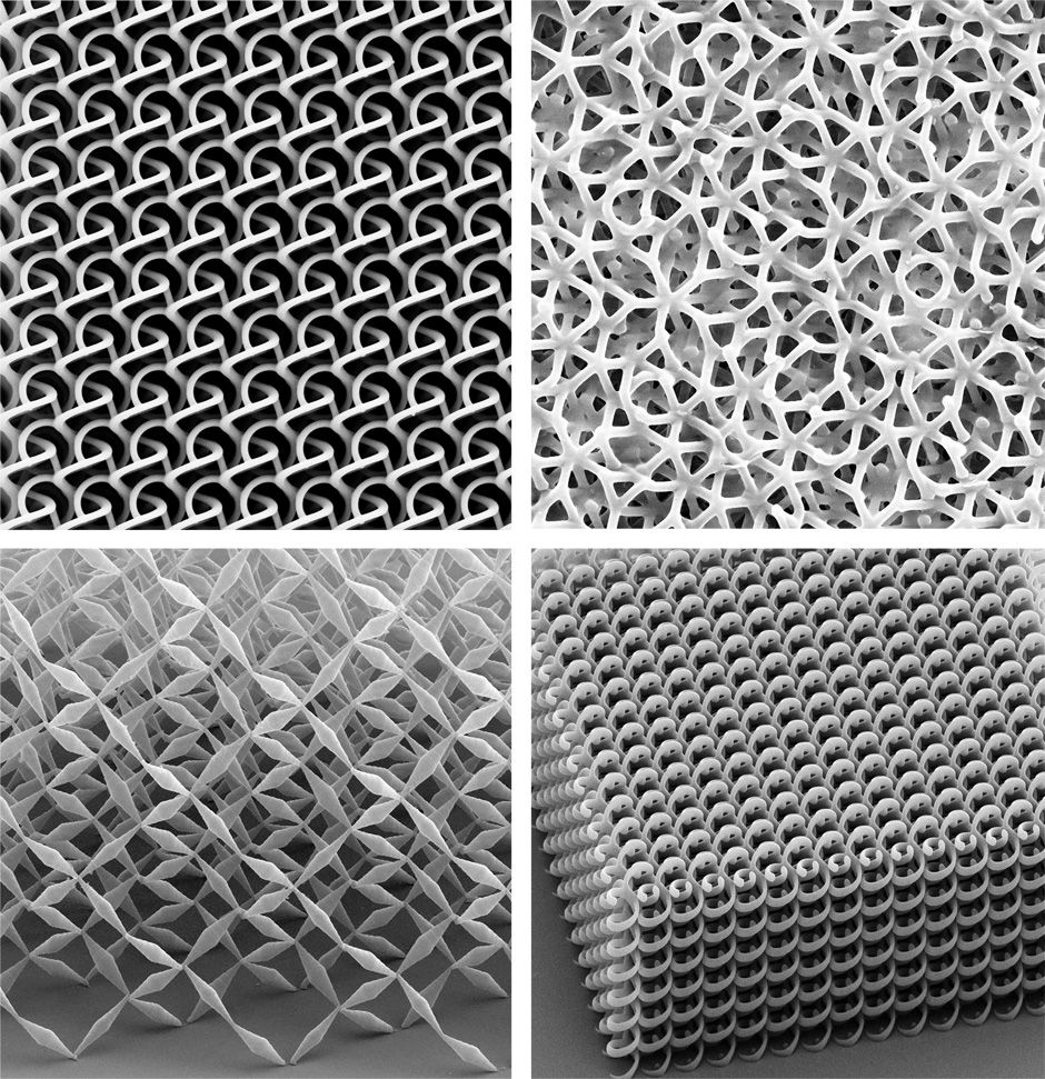
But these lithographic approaches begin to break down when you try to fabricate even seemingly simple 3-D objects, which is what you need for a metamaterial that can act on light regardless of direction. Lithography is designed to pattern 2-D features, so to construct an array of tiny helical coils, for example, you’d have to construct them layer by layer in hundreds of steps. It’s a time-consuming process that requires careful alignment. Even research groups that are adept at the process might need an entire day to make a single layer.
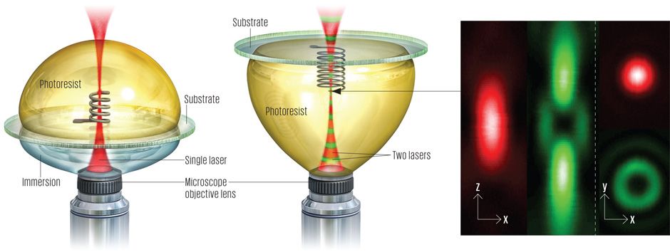
Fortunately, there is a better way to make 3-D structures. The key is to use laser light, and some tricks developed over the last few years, to write in three-dimensional space. You could consider this type of optical lithography—direct laser writing—as a microscopic version of 3-D printing. Just as with rapid prototyping, or stereolithography, which was patented by Charles W. Hull in 1986, light is used to sketch out a shape. In this case, however, shapes are not made layer by layer. Instead they’re all made in one go, out of a single volume of material. Solvent washes away what isn’t exposed to light, much as Michelangelo might say an artist creates a sculpture: by chipping away excess stone.
As in other lithographic techniques, direct laser writing uses a compound called resist—in this case, a photosensitive mixture called photoresist. To make metamaterials, we start with a thick layer of the stuff, which coats a glass slide or some other substrate and is mounted on a microscope. When we shine a laser through the microscope optics and onto the photoresist, the light breaks molecules apart and causes the exposed material to polymerize and harden. When we’re done, we can wash away the unexposed material with solvent, and only the exposed material remains.
Ordinarily, this approach would work well in only two dimensions. That’s because even if we focused the laser deep into the resist, photons would be absorbed not only close to the focal region but also throughout the entire beam cone, below and above the focus. To make the curing process work in three dimensions, we alter the strategy slightly, pairing the “photoinitiator”—the part of the photoresist that absorbs photons—with a longer-wavelength laser. If the combination of the two is just right, we can create a system in which the photoinitiator must absorb two photons instead of one to become excited.
If two photons are needed, the absorption response isn’t linear. Instead, it scales with the square of the light intensity; if we double it, we can get four times the response. That helps confine the effect of a laser: If a laser beam is tightly focused, the exposure will be sharply confined to a small volume around the center of the focus. Then, to draw an arbitrary 3-D shape, we need only move the focus around, by either moving the sample or the laser beam.
All by itself, however, this technique isn’t quite enough to get us meta-atoms small enough to interact with light. The limitation is the Abbe diffraction barrier—a characteristic of microscope optics that limits the spatial resolution of a lens and thus how closely you can put two adjacent features or lines. For an 800-nm laser—which works well with common photoresists—and for high-end microscope lenses, you’re limited to a lateral distance of about 300 nm because of Abbe.
For decades, this limitation appeared to be fundamental. But about five years ago, we proved there was a way past it. The idea got its start with physicist Stefan Hell, now at the Max Planck Institute for Biophysical Chemistry, in Göttingen, Germany. In the early 1990s, he proposed a way to break the diffraction barrier by using a second laser operating with a different frequency.
Through a process called stimulated emission depletion, this second laser can cause an excited molecule to spit out a photon and relax back to a lower energy state. That’s useful for lithography, because, in effect, it gives us an eraser to go with our pen. The writing beam will have a hot spot in the center, and the erasing beam will have a different cross section: a specially shaped focus with zero intensity right where the writing laser is at its maximum [see illustration, "Writing Through Resist"]. When both beams are used, everything outside the very center of the writing beam can be de-excited, and the photoresist there will remain unexposed.
Hell’s group was interested in using this technique to cause stained cells and other biological structures to fluoresce in as tiny a spot as possible, so they could be imaged at very high resolution under the microscope. (His team has since done this to great effect: In 2009, they showed they could resolve features under the microscope as small as 6 nm—just a few atoms across—using visible light, well under the Abbe diffraction barrier.)
But adapting the two-laser approach to curing photoresists wasn’t easy. When our group at KIT started to look into the possibility in 2008, there were no photoresists that had been specifically developed to support the approach. One complication we encountered early on was that photoinitiators are designed to be efficient; after they’re hit by photons, they react in almost no time at all, too fast for a second laser beam to de-excite the molecule and stop the polymerization reaction. It took about a year of research and some trial and error, but we eventually found a photoinitiator—a dye molecule that had been used only sparingly for lithography up until that point—that would do the job.
With that photoinitiator in hand, we found we could print structures with a lateral resolution—the distance between two adjacent features—of about 175 nm, about 40 percent finer than what can be achieved at the Abbe limit.
That’s quite an improvement. But in principle, spatial resolutions of a few tens of nanometers (beyond that you’re starting to reach the molecular scale) should be possible using 800-nm light. Pushing the resolution of this lithography down to such a scale will require more work. The problem is no longer optics; it’s the photoresists that we use. For reasons that are still being explored—perhaps the diffusion of the photoresist molecules themselves—attempts to make smaller structures typically result in ill-defined features. If you try to make two features closer together than 175 nm, for example, you can end up curing areas that aren’t supposed to be part of the final shape.
Still, the resolution is now fine enough to allow us to create artificial materials that can operate in the visible part of the spectrum. Many of them would have been impossible to make even five years ago.
Returning to our favorite example, the invisibility cloak: When we began working on the problem in early 2009, other groups had already succeeded in making structures that could cloak objects in two dimensions. But accomplishing this same feat at optical wavelengths and in three dimensions requires a bit more planning.
For design guidelines, we relied on work done by metamaterials theorists, such as Pendry at Imperial College and Ulf Leonhardt at the University of St. Andrews, in Scotland, who have shown how to reverse engineer a metamaterial design from the properties you want it to have. The trick is to use coordinate transformations, which are a bit like those used to work out how mass distorts the fabric of space-time in Einstein’s general relativity. These let you derive the structure of a metamaterial from the way you want it to affect the flow of light.
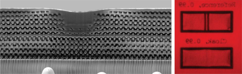
Thanks to direct laser writing, invisibility cloaks that can operate at visible wavelengths have become a reality. We haven’t used them to make anything as large as a person invisible. However, we have used them to alter the appearance of smallish things. The 3-D “carpet cloak” [see images, "Gone in 5 Micrometers"] that we constructed is based on a restricted geometry, but it does work for visible light and over a large range of frequencies, and it can make a patch of curved floor (the carpet) look as if it were a flat metal mirror.
The metamaterials menagerie now includes a number of other creations that previously seemed impossible. Photonic crystals based on titanium dioxide that completely reflect visible light coming from any direction are one recent creation; they could be used to steer light emitted by LEDs. Pentamode mechanical metamaterials—solids that behave much like liquids—have also been made. These could be used to create an unfeelability cloak that yields to pressure, so that the presence of an object can’t be detected by touch. We’ve also succeeded in making 3-D photonic quasicrystals, the optical counterpart to the strange physical structures for which Dan Shechtman won the Nobel Prize in Chemistry in 2011. Although we’re still exploring applications for this exotic material, direct laser writing is the only way to make the complex underlying structures.
In the midst of all this exciting fabrication work, another innovation has drastically changed the fabrication process. Early laser writing was limited by microscope optics: It was necessary for a glass slide to sit between the microscope’s objective lens and the photoresist. That arrangement meant that metamaterials could be no more than about 100 micrometers thick.
But in 2012, a new approach, introduced by Nanoscribe, a company that developed out of research done at our lab, solved this issue. In immersion microscopy, the microscope’s objective lens is coated with a droplet of oil that sits between the lens and a glass slide. Nanoscribe created a special photoresist with the right refractive index to replace that oil, so that the resist could be dropped directly onto the lens.
Without the aforementioned two-photon absorption, of course, this scheme wouldn’t be a good idea at all. Photons coming out of the lens would cure the photoresist all along the beam line, causing the photoresist to stick to the lens and destroying the lens after its first use. But recall that with two-photon absorption, we can localize the curing process in three dimensions.
This “dip-in” approach also enables us to build structures on surfaces other than glass. And because the resist and the lens are no longer separated by a thick glass substrate, we can extend the focus a good 10 times as far into a sample, creating 3-D metamaterials arrays as tall as 1 mm. That’s getting close to a height where we can begin thinking about constructing macroscopic metamaterials—objects that are large enough to hold in your hand—rather than just thin, delicate coatings.
Of course, there’s still room for improvement. The resolution of direct laser writing is only barely sufficient to make light-manipulating metamaterials that can operate at visible frequencies. Some more-complex structures, such as forests of metal helices, are still out of reach, and making them will likely require new photoresists. But in principle at least, there is no obvious reason we won’t succeed.
We’ll also have to tackle the issue of writing speed. On that front, we’ve actually been making good progress. In research labs, the laser is fixed, and structures are drawn by moving the sample around using high-precision 3-D piezoelectric actuators. These are commonly used at speeds of about 100 micrometers per second. For many structures, that translates to half an hour or so of work to create a metamaterial with a 100- by 100-µm footprint. But recently, Nanoscribe and others have adopted 2-D galvanometer-based laser scanning systems that can write much faster, with speeds upwards of 1 meter per second. Using these lithography instruments, which are now commercially available, we can reduce the fabrication times by a factor of a hundred or more.
Metamaterials are just the start. With the recent speed boost and with further improvements to spatial resolution, we think that direct laser writing might one day compete with planar electron-beam lithography, which is used today to make the stencil-like masks that pattern circuits on logic and memory chips.
And there’s more. By incorporating active elements, such as nanodiamonds engineered to emit single photons, we could even envision creating 3-D optical systems for chip-based quantum information processing.
We’re only beginning to explore what can be done with these new fabrication tools. But in the future, there may be no limit to how sophisticated and intricately structured matter can become.
This article originally appeared in print as “Matter Made to Order.”
About the Authors
Metamaterials small enough to work at optical wavelengths were largely theoretical in 2001, when Martin Wegener, a professor at the Karlsruhe Institute of Technology (KIT), in Germany, began working on a way to fabricate them using direct laser writing. Now, he says, “we can fabricate nearly any three-dimensional architecture from scratch.” Coauthor Joachim Fischer is a postdoc in Wegener’s group. Michael Thiel left the lab in 2010 after completing his Ph.D. to join KIT spin-off Nanoscribe, where he currently heads technical development.


