If there’s one thing about Moore’s Law that’s obvious to anyone, it’s that transistors have been made smaller and smaller as the years went on. Scientists and engineers have taken that trend to an almost absurd limit during the past decade, creating devices that are made of one-atom-thick layers of material.
The most famous of these materials is, of course, graphene, a hexagonal honeycomb-shaped sheet of carbon with outstanding conductivity for both heat and electricity, odd optical abilities, and incredible mechanical strength. But as a substance with which to make transistors, graphene hasn’t really delivered. With no natural bandgap—the property that makes a semiconductor a semiconductor—it’s just not built for the job.
Instead, scientists and engineers have been exploring the universe of transition metal dichalcogenides, which all have the chemical formula MX2. These are made up of one of more than a dozen transition metals (M) along with one of the three chalcogenides (X): sulfur, selenium, or tellurium. Tungsten disulfide, molybdenum diselenide, and a few others can be made in single-atom layers that (unlike graphene) are natural semiconductors. These materials offer the enticing prospect that we will be able to scale down transistors all the way to atom-thin components long after today’s silicon technology has run its course.
While this idea is really exciting, I and my colleagues at Imec believe 2D materials could actually show up much sooner, even while silicon still remains king. We’ve been developing a technology that could put 2D semiconductors to work in silicon chips, enhancing their abilities and simplifying their designs.
Devices made with 2D materials are worth all the scientific and engineering work we and other researchers around the world have put into them because they could eliminate one of the biggest problems with today’s transistors. The issue, the result of what are called short-channel effects, is a consequence of the continual shrinking of the transistor over the decades.
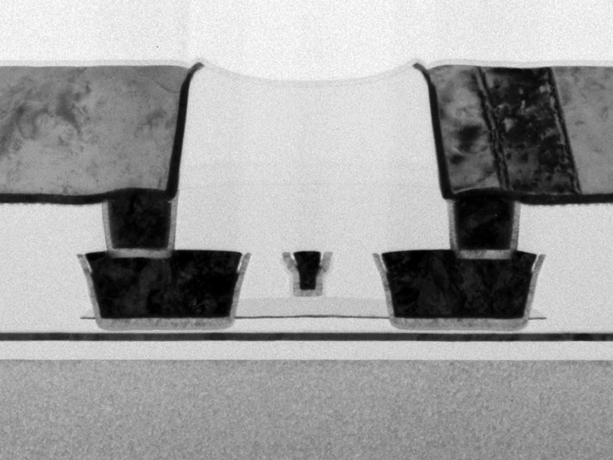
A metal-oxide semiconductor field-effect transistor (MOSFET), the type of device in all digital things, is made up of five basic parts: The source and drain electrodes; the channel region that connects them; the gate dielectric, which covers the channel on one or more sides; and the gate electrode, which contacts the dielectric. Applying a voltage at the gate relative to the source creates a layer of mobile charge carriers in the channel region that forms a conductive bridge between the source and drain, allowing current to flow.
But as the channel was made smaller and smaller, current would increasingly leak across it even when there was no voltage on the gate, wasting power. The change from the planar designs of the 20th century to the FinFET transistor structure used in today’s most advanced processors was an attempt to counter this important short-channel effect by making the channel region thinner and having the gate surround it on more sides. The resulting fin-shaped structure provides better electrostatic control. (The coming move to the nanosheet transistor is a furthering of this same idea. See “The Last Silicon Transistor,” IEEE Spectrum, August 2019.)
Certain 2D semiconductors could circumvent short-channel effects, we think, by replacing the silicon in the device channel. A 2D semiconductor provides a very thin channel region—as thin as a single atom if only one layer of semiconductor is used. With such a restricted pathway for current to flow, there is little opportunity for charge carriers to sneak across when the device is meant to be off. That means the transistor could continue to be shrunk down further with less worry about the consequences of short-channel effects.
These 2D materials are not only useful as semiconductors, though. Some, such as hexagonal boron nitride, can act as gate dielectrics, having a dielectric constant similar to that of silicon dioxide, which was routinely used for that job until about a decade ago. Add graphene in place of the transistor’s metal parts and you’ve got a combination of 2D materials that forms a complete transistor. Indeed, separate groups of researchers built such devices as far back as 2014. While these prototypes were much larger, you could imagine scaling them down to the size of just a few nanometers.
As amazing as an all-2D transistor that’s a fraction of the size of today’s devices might be, that won’t be the first implementation of 2D materials in electronic circuits. Instead, 2D materials will probably arrive in low-power circuits that have more relaxed performance requirements and area constraints.
The set of circuits we’re targeting at Imec are built in the so-called back-end-of-line. Chipmaking is divided into two parts: the front-end-of-line part consists of processes—many of them requiring high temperatures—that alter the silicon itself, such as implanting dopants to define the parts of a transistor. The back-end-of-line part builds the many layers of interconnects that link the transistors to form circuits and deliver power.
With traditional transistor scaling becoming more and more difficult, engineers have been looking for ways to add functionality to the interconnect layers. You can’t do this simply by using ordinary silicon processes because the heat involved would damage the devices and interconnects beneath them. So, many of these schemes rely on materials that can be made into devices at relatively low temperatures.

A specific advantage of using 2D semiconductors instead of some other candidates is the potential ability to build both p-type (carrying positive charges) and n-type (carrying electrons) devices, a necessity in CMOS logic. CMOS circuits are the backbone of today’s logic because, ideally, they consume power only when switching from one state to the other. In our preferred 2D semiconductor, we’ve demonstrated n-type transistors but not yet p-type. However, the physics underlying these materials strongly suggests we can get there through engineering the dielectrics and metals that contact the semiconductor.
Being able to produce both p- and n-type devices would allow the development of compact back-end logic circuits such as repeaters. Repeaters essentially relay data that must travel relatively far across a chip. Ordinarily, the transistors involved reside on the silicon, but that means signals must climb up the stack of interconnects until they reach a layer where they can travel part of the distance to their destination, then go back down to the silicon to be repeated and up again to the long-distance interconnect layer. It’s a bit like having to exit the highway and drive into the center of a crowded city to buy petrol before getting back on the highway.
A repeater up near the long-distance interconnect layer is more akin to a motorway petrol station. It saves the time it would take the signal to make the two-way vertical trip and also prevents the loss of power due to the resistance of the vertical interconnects. What’s more, moving the repeater to the interconnect layer saves space on the silicon for more logic.
Repeaters aren’t the only potential use. A 2D material could also be used to build other circuits, such as on-chip power-management systems, signal buffers, and memory selectors. One thing these circuits all have in common is that they don’t require the device to drive a lot of current, so one layer of 2D material would probably be sufficient.
Neither future supersmall 2D devices nor the less demanding back-end-of-line circuits will be possible without a fabrication process compatible with industry-standard 300-millimeter silicon wafers. So our team at Imec is working on just that, hoping to develop a process that will serve for all applications.
The first step is identifying the most promising 2D material and device architecture. We have therefore benchmarked a variety of 2D semiconductors and 2D FET architectures against an advanced silicon FinFET device.
Because researchers have the most experience with molybdenum disulfide (MoS2), experimental devices made using it have advanced furthest. Indeed, at the IEEE International Electron Device Meeting last December, Imec unveiled an MoS2 transistor with a channel just 30 nanometers across and source and drain contacts only 13 nm long. But after examining the possibilities, we’ve decided that MoS2 is not the answer. Instead, we concluded that among all the materials compatible with 300-mm silicon-wafer technology, tungsten disulfide (WS2) in the form of a stacked nanosheet device has the highest performance potential, meaning it can drive the most current. For less demanding, back-end-of-line applications, we also concluded that a FET architecture with a gate both below and above the semiconductor channel region works better than one with only a single gate.
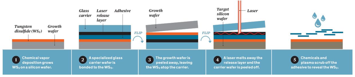
We already knew one important thing about WS2 before we reached that conclusion: We can make a high-quality version of it on a 300-mm silicon wafer. We demonstrated that for the first time in 2018 by growing the material on a wafer using metal-organic chemical vapor deposition (MOCVD), a common process that grows crystals on a surface by means of a chemical reaction. The approach we took results in thickness control down to a single-molecule layer, or monolayer, over the full 300-mm wafer. The benefits of the MOCVD growth come, however, at the price of a high temperature—and recall that high temperatures are forbidden in back-end processes because they could damage the silicon devices below.
To get around this problem, we grow the WS2 on a separate wafer and then transfer it to the already partially fabricated silicon wafer. The Imec team developed a unique transfer process that allows a single layer of WS2—as thin as 0.7 nm—to be moved to a silicon target wafer with negligible degradation in the 2D material’s electrical properties.
The process starts by growing the WS2 on an oxide-covered silicon wafer. That’s then placed in contact with a specially prepared wafer. This wafer has a layer of material that melts away when illuminated by a laser. It also has a coating of adhesive. The adhesive side is pressed to the WS2-covered wafer, and the 2D material peels away from the growth wafer and sticks to the adhesive. Then the adhesive wafer with its 2D cargo is flipped over onto the target silicon wafer, which in a real chipmaking effort would already have transistors and several layers of interconnect on it. Next, a laser is shone through the wafer to break the bulk of it away, leaving only the adhesive and the WS2 atop the target wafer. The adhesive is removed with chemicals and plasma. What’s left is just the processed silicon with the WS2 attached to it, held in place by Van der Waals forces.
The process is complicated, but it works. There is, of course, room for improvement, most importantly in mitigating defects caused by unwanted particles on the wafer surface and in eliminating some defects that occur at the edges.
Once the 2D semiconductor has been deposited, building devices can begin. On that front there have been triumphs, but some major challenges remain.
Perhaps the most crucial issue to tackle is the creation of defects in the WS2. Imperfections profoundly degrade the performance of a 2D device. In ordinary silicon devices, charge can get caught in imperfections at the interface between the gate dielectric and the channel region. These can scatter electrons or holes near the interface as they try to move through the device, slowing things down. With 2D semiconductors the scattering problem is more pronounced because the interface is the channel.

Sulfur vacancies are the most common defects that affect device channel regions. Imec is investigating how different plasma treatments might make those vacancies less chemically reactive and therefore less prone to alter the transistor’s behavior. We also need to prevent more defects from forming after we’ve grown the monolayer. WS2 and other 2D materials are known to age quickly and degrade further if already defective. Oxygen attacking a sulfur vacancy can cause more vacancies nearby, making the defect area grow larger and larger. But we’ve found that storing the samples in an inert environment makes a difference in preventing that spread.
Defects in the semiconductor aren’t the only problems we’ve encountered trying to make 2D devices. Depositing insulating materials on top of the 2D surface to form the gate dielectric is a true challenge. WS2 and similar materials lack dangling bonds that would otherwise help fasten the dielectric to the surface.
Our team is currently exploring two routes that might help: One is atomic layer deposition (ALD) at a reduced growth temperature. In ALD, a gaseous molecule adsorbs to the semiconductor’s exposed surface to form a single layer. Then a second gas is added, reacting with the adsorbed first one to leave an atomically precise layer of material, such as the dielectric hafnium dioxide. Doing this at a reduced temperature increases the ability of the gas molecules to stick to the surface of the WS2 even when no chemical bonds are available.
The other option is to enhance ALD by using a very thin oxidized layer, such as silicon oxide, to help nucleate the growth of the ALD layer. A very thin layer of silicon is deposited by a physical deposition method such as sputtering or evaporation; it’s then oxidized before a regular ALD deposition of gate oxide is done. We’ve achieved particularly good results with evaporation.
A further challenge in making superior 2D devices is in choosing the right metals to use as source and drain contacts. Metals can alter the characteristics of the device, depending on their work function. That parameter, the minimum energy needed to extract an electron from the metal, can mean the difference between a contact that can easily inject electrons and one that can inject holes. So the Imec team has screened a variety of metals to put in contact with the WS2 nanosheet. We found that the highest on-current in an n-type device was obtained using a magnesium contact, but other metals such as nickel or tungsten work well. We’ll be searching for a different metal for future p-type devices.
Despite these challenges, we’ve been able to estimate the upper limits of device performance, and we’ve mapped out what roads to follow to get there.
As a benchmark, the Imec team used dual-gated devices like those we described earlier. We built them with small, naturally exfoliated flakes of WS2, which have fewer defects than wafer-scale semiconductors. For these lab-scale devices, we were able to measure electron mobility values up to a few hundred square centimeters per volt-second, which nearly matches crystalline silicon and is close to the theoretically predicted maximum for the 2D material. Because this excellent mobility can be found in natural material, we are confident that it should also be possible to get there with materials synthesized on 300-mm wafers, which currently reach just a few square centimeters per volt-second.
For some of the main challenges ahead in 2D semiconductor development, our team has a clear view of the solutions. We know, for example, how to grow and transfer the material onto a 300-mm target wafer; we’ve got an idea of how to integrate the crucial gate dielectric; and we’re on a path to boost the mobility of charge carriers in devices toward a level that could compare with silicon.
But, as we’ve laid out, there are still significant problems remaining. These will require an intensive engineering effort and an even better fundamental understanding of this new class of intriguing 2D materials. Solving these challenges will enable high-performance devices that are scaled down to atomic layers, but they might first bring new capabilities that need less demanding specifications even as we continue to scale down silicon.
This article appears in the February 2020 print issue as “Atom-Thick Transistors.”