All-ar

Our always-on world of PCs, tablets, and smartphones has come about because of one remarkable trend: the relentless miniaturization of the metal-oxide-semiconductor field-effect transistor, or MOSFET. This device, which is the building block of most integrated circuits, has shrunk a thousandfold over the past half century, from the tens-of-micrometers scale in the 1960s to tens of nanometers today. And as the MOSFET has become tinier, generation after generation, the chips based on it have become much faster and less power hungry than their predecessors.
This trend has given rise to one of the longest and greatest winning streaks in industrial history, bringing us gadgets, capabilities, and conveniences that previous generations could scarcely have imagined. But now this steady progress is under threat. And at the heart of the problem lies quantum mechanics.
The electron has a pesky ability to penetrate barriers—a phenomenon known as quantum tunneling. As chipmakers have squeezed ever more transistors onto a chip, transistors have gotten smaller, and the distances between different transistor regions have decreased. So today, electronic barriers that were once thick enough to block current are now so thin that electrons can barrel right through them.
Chipmakers have already stopped thinning one key transistor component—the gate oxide. This layer electrically separates the gate, which turns a transistor on and off, from the current-carrying channel. Make this oxide thinner and you can induce more charge in the channel, boost the current, and make the transistor faster. But you can't reduce the oxide thickness to much less than roughly a nanometer, which is about where it is today. Beyond that, too much current will flow across the channel when the transistor is “off," when ideally no current should flow at all. And that's just one of several leakage points.
It has long been hard to pin down the precise year when size reductions will end. Industry road maps now project the miniaturization of the MOSFET out to 2026, when gates will be just 5.9 nanometers long—about a quarter the length they are today. This timeline assumes that we'll be able to find better materials to stanch leaks. But even if we do, we'll need to find a replacement for the MOSFET soon if we want to continue getting the performance enhancements we're used to.
We can't stop electrons from tunneling through thin barriers. But we can turn this phenomenon to our advantage. In the last few years, a new transistor design—the tunnel FET, or TFET—has been gaining momentum. Unlike the MOSFET, which works by raising or lowering an energy barrier to control the flow of current, the TFET keeps this energy barrier high. The device switches on and off by altering the likelihood that electrons on one side of that barrier will materialize on the other side.

That's a huge departure from the way traditional transistors work. But it might be just the thing to pick up where the MOSFET leaves off, paving the way for faster, denser, and more energy-efficient circuits that will extend Moore's Law well into the next decade.
It wouldn't be the first time the transistor has changed form. Initially, semiconductor-based computers used circuits made from bipolar transistors. But only a few years after the silicon MOSFET was demonstrated in 1960, engineers realized they could make two complementary switches. These could be combined to make complementary metal-oxide-semiconductor (CMOS) circuits that, unlike bipolar transistor logic, consumed energy only while switching. Ever since the first integrated circuits based on CMOS emerged in the early 1970s, the MOSFET has dominated the marketplace.
In many ways, the MOSFET wasn't a big departure from the bipolar transistor. Both control the current flow by raising and lowering energy barriers—a bit like raising and lowering a floodgate in a river. The “water" in this case consists of two kinds of current carriers: the electron and the hole, a positively charged entity that's essentially the absence of an electron in the outer energy shell of an atom in the material.
There are two allowable energy ranges, or bands, for these charge carriers. Electrons with enough energy to flow freely through the material are in the conduction band. Holes flow in a lower-energy band, called the valence band, and they move from atom to atom, much as an empty parking space might migrate around a nearly full parking lot as neighboring cars pull in and out.
These bands are fixed, but we can shift the energies associated with them up or down by adding impurities, or dopant atoms, to alter the conductivity of the semiconductor. N-type semiconductors, which are doped to contain an excess of electrons, conduct negatively charged electrons; p-type semiconductors, which are doped to produce a deficit of electrons, conduct positively charged holes.
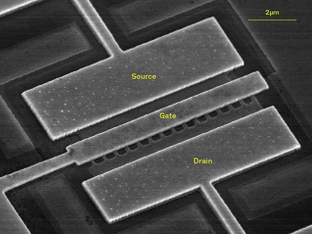
If we put these two semiconductor types together, we get a junction with bands that are misaligned, thus creating an energy barrier between them. To make a MOSFET, we insert one type of material between two of the complementary type, in either an n-p-n or a p-n-p configuration. This creates three regions in the transistor: the source, where charges enter the device; the channel; and the drain, where they exit.
The two p-n junctions in each transistor provide electronic barriers to the flow of charges, and the transistor can be switched on by applying a voltage to the gate on top of the channel. A positive voltage applied to an n-channel MOSFET gate makes the channel more attractive to electrons, because it decreases the amount of energy an electron needs to have in order to move into the channel. A negative voltage applied to a p-channel MOSFET gate will perform the same task for holes.
This simple barrier-lowering strategy is the most widely used current-control mechanism in semiconductor electronics. Diodes, lasers, bipolar transistors, thyristors, and most field-effect transistors all take advantage of it. But it has a physical limit: Transistors need a certain amount of voltage to be switched on or off. This arises from the fact that electrons and holes are in constant motion due to their thermal energy, and the most energetic among them spill over the barrier. At room temperature, the current flowing over the barrier increases by a factor of 10 when the energy barrier is lowered by 60 millivolts; every “decade" of current change requires a change of 60 mV.
All this current leakage occurs below the device's threshold voltage, which is the voltage needed for the transistor to turn on. Device physicists call this barrier-lowering region the subthreshold region, and 60 mV per decade is known as the minimum subthreshold swing. To keep power consumption down, subthreshold swing should be as low as possible. The device will then need less voltage to be switched on, and it will leak less current when it's off.

Subthreshold swing wasn't much of an issue in the past, in the days when chips ran with higher voltages. But now it's starting to interfere with our ability to drive down power. That's partly due to the fact that circuit designers want to make sure their logic components have a big difference between the current that is used to define a “0" and the current that defines a “1." Transistors are typically designed so that when they're on they carry about 10 000 times as much current as they leak when they're off. That means at least 240 mV must be applied to the transistor to turn it on: four decades of current, each decade requiring at least 60 mV.
In practice, the operating voltages used in CMOS circuits are typically much higher, closer to 1 volt. That's because the fundamental logic circuit in CMOS, the inverter, uses two transistors in series. The NAND gate takes three transistors in series, which means it requires even more voltage than the inverter. If you adjust for process variability—which means you need to set wider voltage margins to account for variations from device to device—you arrive at the voltages needed today to guarantee operation.
These voltage requirements, coupled with the leakage problems, mean we're in the waning days of MOSFET miniaturization. There's no way around it. If we want to lower voltage further to cut down on power consumption, we have two equally unattractive options. We can lower the current we drive through the device, which lowers the switching speed and thus sacrifices performance, or we can keep the current high and allow more current to leak through the device when it's supposed to be off.
That's where the tunnel FET comes in. Instead of raising or lowering the physical barrier between the source and drain as you would in a MOSFET, we use the gate to control the effective, electrical thickness of the barrier and thus the probability that electrons can slip through it.

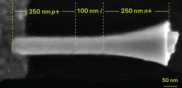
The trick to doing this is again the p-n junction—with a bit of a twist. In a TFET, we arrange semiconducting material in p-i-n and n-i-p configurations. The i stands for “intrinsic," and it means that the channel has as many electrons as there are holes. The intrinsic state corresponds to the maximum resistivity that a semiconductor can have. It also pushes up the energies associated with the bands in the channel, introducing a thick energy barrier that charge carriers in the source are unlikely to traverse.
Electrons and holes obey the laws of quantum mechanics, which means they have a fuzzy, uncertain size. When an energy barrier has a thickness below about 10 nanometers, there is a small but nonzero probability that an electron that starts on one side of the barrier will appear on the other.
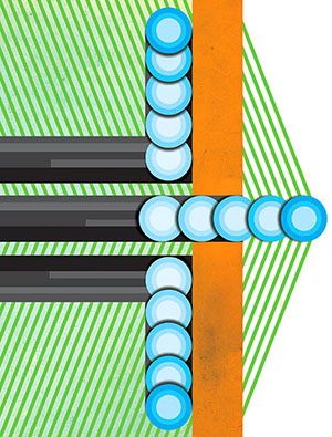
In the TFET, we boost this probability by applying a voltage to the transistor gate. This causes the conduction band in the source and the valence band in the channel to overlap, opening up a tunneling window. Note that in a TFET, the electrons tunnel between conduction and valence bands as they move into the channel. This is in contrast to what happens in a MOSFET, in which electrons or holes travel primarily in either one band or the other all the way from source to channel to drain.
Because the tunneling mechanism isn't controlled by the flow of carriers over a barrier, TFETs should be able to switch with a much smaller voltage swing than that required in a MOSFET. You have to apply only enough voltage to create or remove an overlap, crossing and uncrossing the bands [see bottom half of illustration "Off and On", above].
As a device mechanism, tunneling is not a new idea. The flash memory inside our USB sticks, cellphones, and other gadgets uses tunneling to inject electrons across oxide barriers into charge-trapping regions. Tunnel junctions like the one used in the TFET are also widely used to connect multijunction solar cells and to trigger semiconductor-based quantum cascade lasers. And tunneling governs the way current flows across metal-semiconductor contacts, an essential part of every semiconductor device.
The p-n tunnel junction has also been around a while. It was first demonstrated and explained by Nobel Prize winner Leo Esaki in 1957. But it took a fundamental impediment to get the industry to think seriously about how tunneling might be applied to logic.

The first TFET papers were written only about nine years ago, when chipmakers started to see computer clock speeds stall and struggled with the problem of removing heat from denser, leakier chips.
Joerg Appenzeller and his colleagues at IBM were the first to demonstrate that current swings below the MOSFET's 60-mV-per-decade limit were possible. In 2004, they reported they had created a tunnel transistor with a carbon nanotube channel and a subthreshold swing of just 40 mV per decade. Within a few years, groups at UC Berkeley, CEA-Leti, Imec, and Stanford had followed suit. They showed that switches that consume less than 60 mV per decade could be made using semiconducting materials that are staples of the chip industry: silicon and germanium.
That got the community excited, because although the current-control mechanism in the TFET is new to the semiconductor industry, the device bears a strong resemblance to the MOSFET. It has the same basic configuration of source, drain, and gate and similar electrical behavior when wired into circuits. The semiconductor design infrastructure does not need to change.
But some changes are required. It turns out that silicon and germanium aren't great for tunneling. It's for the same reason that these materials don't make good light emitters and lasers. Silicon and germanium have indirect bandgaps, which means that in order to transition from one band to another, electrons must also absorb some extra energy from vibrations in the crystal lattice that makes up the material. This extra hurdle significantly lowers the probability that charge carriers will make the leap. As a result, the current-carrying capacity of silicon and germanium TFETs is only a trickle compared with that of today's transistors.
That might be a stumbling block for adoption by the industry. However, there are a range of direct-bandgap materials, based on a mix of elements picked from columns III and V of the periodic table, that have considerably higher tunneling probabilities. These materials have yet to make it into mass production in logic chips, but work on incorporating them into traditional MOSFETs is already gearing up [see “ Changing the Channel," IEEE Spectrum, July 2013]. The notion that they might emerge in logic chips in the foreseeable future is not nearly as far-fetched as it would have seemed just a few years ago.
Research into TFETs made from III-V materials has also been advancing rapidly in recent years. Suman Datta and his colleagues at Pennsylvania State University were the first to demonstrate III-V TFETs, in 2009. They used channels made of a mix of indium, gallium, and arsenic and immediately set a record, with an “on" current that was 50 times as high as with the best germanium TFET.
Since then, the Penn State team and my group at the University of Notre Dame, in South Bend, Ind., have both shown even higher currents in TFETs made from a mix of two compounds: aluminum gallium antimonide and indium arsenide. The former material has bands that can be shifted up or down by tuning the ratio of aluminum to gallium. This lets us create tunnel junctions that have a natural overlap between bands, which means less voltage is needed to turn them on. And because the barrier can be quite thin—just a single atom or so wide—they permit more current. The devices we have built perform well at just 0.5 V and can carry nearly 200 microamperes across a 1-micrometer-wide channel, comparable to what can be accomplished with a state-of-the-art MOSFET.
The one caveat is the subthreshold swing of these “heterojunction" TFETs, which so far hasn't been able to beat the 60-mV-per-decade limit for the MOSFET. Many research groups are now struggling with this challenge. The main culprit is defects—many of which arise from dangling chemical bonds—at the interface between the semiconductor and gate oxide. These defects trap and immobilize charges, leaving fewer charges available for conduction. This means we have to apply a greater voltage to the gate to induce charge carriers in the channel.
That said, there is reason for optimism. Groups based at Intel, in Hillsboro, Ore., and Hokkaido University, in Sapporo, Japan, have demonstrated III-V TFETs with subthreshold swings of less than 60 mV per decade. And simulations from Intel suggest that it's possible to drive down subthreshold swing even further without monumental changes in materials, simply by scaling down the transistors they have already built. In principle, devices with subthreshold swings of around 20 mV per decade appear possible; the ultimate limit will be set by thermal vibrations in the crystal, which make the edges of the conduction and valence bands less sharp.

Much as it would have been hard to predict the MOSFET's ultimate capabilities 50 years ago, it's difficult to say exactly what may ultimately be achieved with the TFET.
One uncertainty is the maximum current a TFET can carry when it's on. On-current is what ultimately determines the maximum speed of circuits, and for a long time, researchers thought it might be fairly low. But in 2010, Siyu Koswatta at IBM showed in simulation that gallium antimonide and indium arsenide could potentially carry 1900 µA per micrometer of channel width when supplied with just 0.4 V. If such a device could be built, it would compete directly with the MOSFET in high-performance applications. The International Technology Roadmap for Semiconductors targets a current of 1685 µA per micrometer of channel width, at a voltage of 0.73 V.
We will also have to tackle the issue of current leakage when the TFET is in its off state. As the channel gets shorter and shorter, it will be easier for electrons to tunnel directly from the source into the drain.
Figuring out the ultimate limits of the device will depend on such factors as electronic structure, defects, and performance requirements. Fortunately, computational tools developed over the past five years at Purdue University and at ETH Zurich now allow researchers to simulate entire devices, atom by atom and bond by bond, to predict device behavior. This activity is helping to guide experiments.
While the TFET's electrical characteristics look promising, there are also quite a few practical things we must tackle before we can start building chips with these transistors. Researchers have been focusing most of their energy on developing n-channel TFETs. P-channel TFETs—and a complementary process technology that could pair the two transistor types to make circuits—are still on the drawing board.
And chipmakers still have to find ways to address the problem of variability. As MOSFETs shrink, the placement and concentration of dopants and the roughness of interfaces can lead to significant variability in electronic properties. TFETs—which will likely be even smaller than MOSFETs when they're introduced—won't be immune to this problem. As with the MOSFET, we will have to develop other approaches in parallel, such as redundancy and error correction, to address this issue.
Still, I am optimistic that there are more promising results to come. It took just 10 years to get from the first silicon MOSFET to the first CMOS microprocessor. The jump to the TFET is arguably a much bigger challenge. But with more than half a century of experience with semiconductors under our belts, it might come about quicker than we think.
About the Author
An IEEE Fellow and a professor of electrical engineering at the University of Notre Dame, Alan Seabaugh entered the field in the late 1980s, when he worked at Texas Instruments. “The aim was to leapfrog Moore's Law, but we kept getting run over by silicon technology," he says. “Today, the rules are changing."