Electronics enthusiasts like being able to make things themselves. In IEEE Spectrum’s Hands On column, we’ve detailed how readers can make their own solder reflow ovens, conductive ink, and synthetic aperture radars. But making DIY integrated circuits seemed impossibly out of reach. After all, building a modern fab is astronomically expensive: For example, in 2017 Intel announced it was investing US $7 billion to complete a facility for making chips with 7-nanometer-scale features. But Sam Zeloof was not deterred. This 17-year-old high school student has started making chips in his garage, albeit with technology that’s a few steps back along the curve of Moore’s Law.
Zeloof says he has been working on his garage fab, located in his home near Flemington, N.J., for about a year. He began thinking about how to make chips as his “way of trying to learn what’s going on inside semiconductors and transistors. I started reading old books and old patents because the newer books explain processes that require very expensive equipment.”
A key moment came when Zeloof found Jeri Ellsworth’s YouTube channel, where she demonstrated how she had made some home-brew silicon transistors a few years ago. “After I saw [Ellsworth’s] videos I started to make a plan of how I could actually start to do this.”
It took Zeloof about three months to replicate Ellsworth’s transistors. “That was getting my feet wet and learning the processes and everything, and acquiring all the equipment,” he says. “My goals from there were to build on what she did and make actual ICs.” So far, he has made only simple integrated circuits with a handful of components, but he is aiming to build a clone of the ur-microprocessor, the Intel 4004, released in 1971. “It’s got about 2,000 transistors at 10 micrometers.... I think that’s very attainable,” says Zeloof.


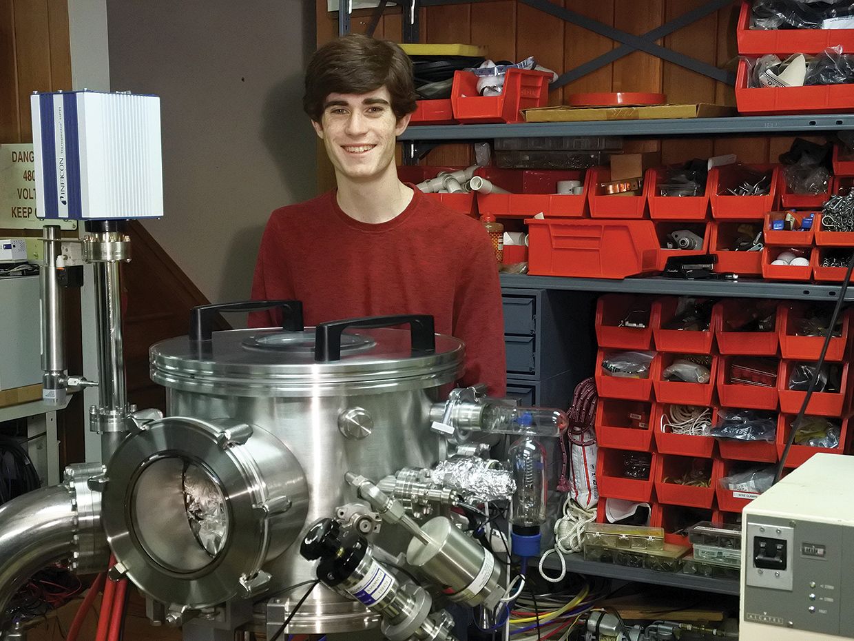
He obtained much of his raw materials and equipment from online sellers, in various states of repair. “Acquiring all the equipment and building and fixing all the stuff I take off eBay is half of the whole journey,” he says. His equipment includes a high-temperature furnace, a vacuum chamber built from surplus parts, and a scanning electron microscope. The electron microscope was “a broken one from a university that just needed some electrical repairs,” says Zeloof. He estimates that the microscope originally cost about $300,000 back in 1996. It was listed for sale at $2,500, but Zeloof persuaded the seller to take “well below that” and ended up spending more on shipping than it cost to buy the microscope.
To pattern the circuits on his chips, Zeloof uses a trick not available in the 1970s: He’s modified a digital video projector by adding a miniaturizing optical stage. He can then create a mask as a digital image and project it onto a wafer to expose a photoresist. With his current setup Zeloof could create doped features with a resolution of about 1 µm, without the time and expense of creating physical masks (however, without a clean-room setup to prevent contamination, he says 10 µm is the limit for obtaining a reasonable yield of working devices). The scanning electron microscope then comes in handy as a diagnostic tool: “I can tell instantly, ‘Oh, it’s overdeveloped. It’s underdeveloped. I have an undercut. I have this. I have that. I have particles that are going to short out the gate area.’ ”
Since he started blogging about his project in 2017, Zeloof has received a lot of positive feedback, including helpful tips from veteran engineers who remember the kind of processes used in the early 1970s. Zeloof hopes that if he can develop a relatively straightforward process for making his 4004 clone, it will open the door for other chips of his own design. “If all goes well, maybe I could make chips for people in the [maker] community—in small batches.”
This article appears in the January 2018 print issue as “The Garage Fab.”