
 Photo: Fritz Goro/The Life Picture Collection/Getty Images
In 1958, 11 years after Bell Labsreinvented the transistor, it became clear that semiconductors would be able to conquer the electronics market only if they could be greatly miniaturized. There wasn’t much progress to be made by hand soldering separate components into circuits, but as is often the case, the solution came just when it was needed.
In July, Jack S. Kilby of Texas Instruments came up with the monolithic idea. His patent application described it as “a novel miniaturized electronic circuit fabricated from a body of semiconductor material containing a diffused p-n junction wherein all components of the electronic circuit are completely integrated into the body of semiconductor material.” And Kilby stressed that “there is no limit upon the complexity or configuration of circuits which can be made in this manner.”
The idea was perfect, but its execution, as depicted in Kilby’s February 1959 patent application, was unworkable because the wire connections arched above the wafer’s surface. Kilby knew that this wouldn’t work, and that is why he added a note about connections to be made in other ways. As an example, he mentioned gold deposited on the thin silicon oxide layer on the wafer’s surface.
Unbeknownst to him, a few months later, in January 1959, Robert Noyce, then the director of research at Fairchild Semiconductor Corp., was to jot in his lab notebook an improved version of the very same idea. “It would be desirable to make multiple devices on a single piece of silicon, in order to be able to make interconnections between devices as part of the manufacturing process, and thus reduce size, weight, etc. as well as cost per active element,” Noyce wrote. Moreover, the drawing accompanying Noyce’s July 1959 patent application contained no flying wires; instead it clearly depicted a planar transistor and “leads in the form of vacuum-deposited or otherwise formed metal strips extending over and adherent to the insulating oxide layer for making electrical connections to and between various regions of the semiconductor body without shorting the junctions.”
Noyce’s patent was granted in April 1961, Kilby’s in July 1964. The litigation went all the way to the Supreme Court, which in 1970 refused to hear the case, upholding a lower court’s ruling of Noyce’s priority. That decision made no practical difference because in 1966 the two companies had agreed to share their production licenses, and the origins of the integrated circuit became yet another outstanding example of concurrent independent inventions. The basic conceptual idea was identical; both inventors received the National Medal of Science, and both were inducted into the Inventor’s Hall of Fame. Noyce lived only to 62, but Kilby survived to share a Nobel Prize for physics in 2000 at the age of 82, five years before his death.
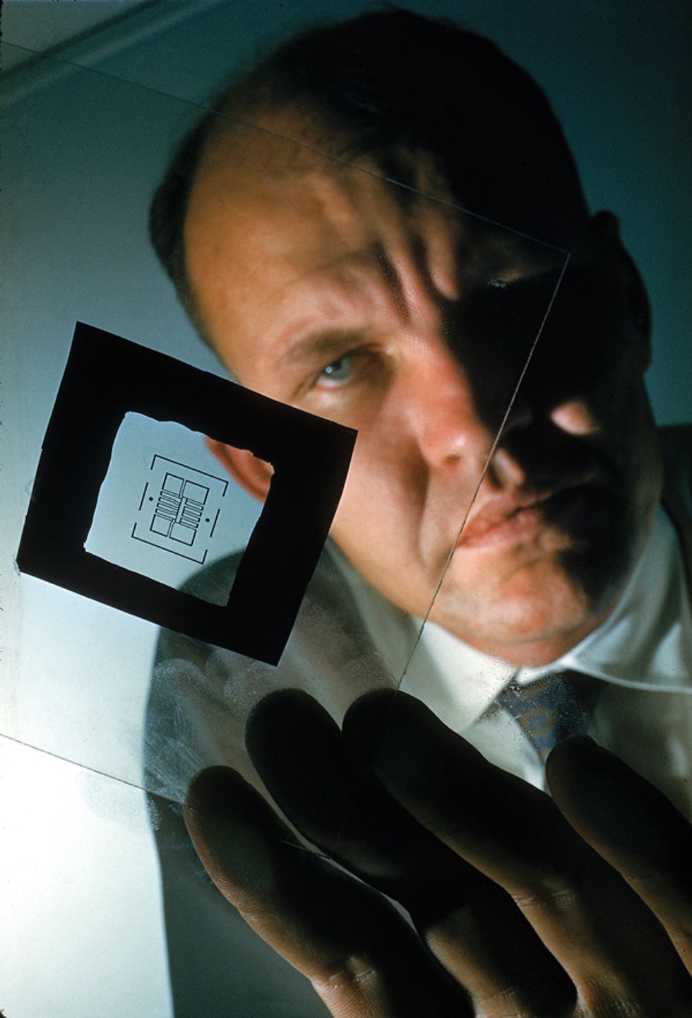
Texas Instruments called the new designs Micrological Elements. They were chosen to control intercontinental ballistic missiles and to help land men on the moon.
Their subsequent progress, captured by the still-enduring Moore’s Law, has been one of the defining developments of our time. By 1971, basic integrated circuits had matured into simple microprocessors with thousands of components, then advanced to designs that made personal computing affordable, starting in the mid-1980s. By 2003, the component total had surpassed 100 million, and by 2015 the SPARC architecture had reached 10 billion transistors. That represents an aggregate growth of eight orders of magnitude since 1965, averaging about 37 percent a year, with the number of components on a given area doubling about every two years. Today you can fit a 6-transistor SRAM cell in an area of .027 square micrometers. As Richard Feynman famously said, there’s plenty of room at the bottom.
Worldwide, semiconductor sales have reached about US $350 billion a year. That’s about 7 million square meters of silicon wafers—about the size of Gibraltar.