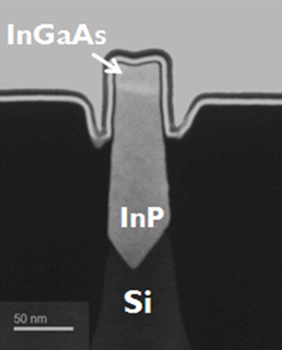
 It’s Groovy: FinFETs are formed by etching a trench with a V-shaped groove in silicon before filling in this hole with indium phosphide and indium gallium arsenide.Image: Imec
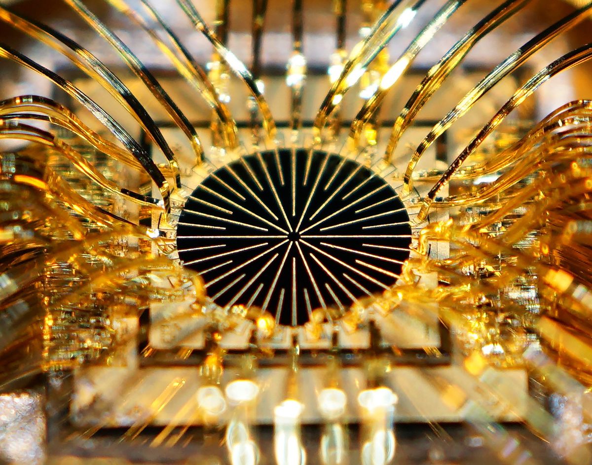
Engineers at the European R&D center Imec have taken a key step toward manufacturing the next decade’s most-advanced chips. On an industry-standard 300-millimeter silicon wafer, they formed FinFETs—the type of 3-D transistor in the most-advanced microprocessors—with a key component built not from silicon but from compound semiconductors.
Building the transistor channel from a compound semiconductor instead of silicon is what many believe will allow chipmakers to continue offering faster and more-complex integrated circuits. By doing it on a 300-mm silicon wafer, Imec has proven that foundries may be able to implement the scheme at an industrial scale.
“This opens up more opportunity and possibility for Moore’s Law,” says Aaron Thean, director of Imec’s R&D program on logic devices. The improvement in efficiency traditionally associated with every new transistor node is under threat. But Imec engineers believe its development will allow this level of progress to be maintained into the next decade.
Transistor efficiency improves with reductions in operating voltage that do not compromise the flow of current through the transistor channel. Straining the channel, essentially elongating the semiconductor crystal, is one way to do this: It allows electrons to zip through silicon up to 70 percent faster, and so lets designers lower the voltage while maintaining current.
But this trick is far harder to perform in the latest incarnation of the silicon transistor, the FinFET, which Intel introduced in 2011 to prevent leakage currents from escalating to an unacceptable level.
“The volume of material in FinFETs is far lower than it is in planar devices, and that means it is harder to strain them,” explains Thean. Instead, engineers are looking to use materials through which charge flows more quickly than in silicon.
With charge-carrier mobility more than six times that of silicon, indium gallium arsenide is a great choice for speeding electrons through the channel, researchers are finding. Dean Freeman, an analyst at Gartner, believes that this type of channel could even make its debut at the 7-nanometer node, the generation of chips due to market in as little as four years. “I don’t want to put words in Intel’s mouth, but there is a potential that we could see this FinFET technology emerge into very high-end servers.”
Smartphones could also benefit, with this new class of FinFET increasing battery life and reducing the number of chips in a phone. Today, in most cases, a mobile phone uses a circuit made from a compound semiconductor to amplify wireless signals and a separate silicon chip to process the data. Imec’s breakthrough could change all that, with both tasks carried out on a single chip.
To convince foundries to make the switch from silicon to indium gallium arsenide FinFETs, Imec’s engineers have developed a relatively low-cost process. Rather than beginning by depositing a blanket of a compound semiconductor across a silicon wafer, an approach used by many researchers in this field, Imec’s engineers begin by growing the high-mobility materials in trenches in the silicon, just tens of nanometers wide.
The profile at the bottom of these tiny trenches plays a crucial role in determining FinFET performance. If compound semiconductors were deposited directly onto a flat surface of a silicon wafer, the resulting film would be rife with metallic bonds between identical atoms that would cause the transistor to short-circuit.
Imec’s engineers eradicate these bonds by growing the crystal on a different crystalline plane, formed by cutting V-shaped grooves into the bottom of the trenches. To minimize leakage current, the trench is filled with indium phosphide before indium gallium arsenide is added to form the protruding fin.
Turning to a trench also reduces defects in the transistor channel. Depositing indium phosphide on silicon always leads to defects, because of the 8 percent difference in average spacing of the atoms in these two crystals. However, these defects—missing planes of atoms aligned at about 45 degrees to the wafer surface—terminate at the trench walls, enabling the growth of high-quality material near the wafer surface.
“I do not want to claim that [the channel] is completely defect-free,” says Thean, “but it’s definitely good enough for the transistor to work now.” He says that the indium gallium arsenide device is almost as good as one made from silicon, while its operating voltage is around half that of a similar silicon FinFET.
The only major weakness of the indium gallium arsenide transistor is its trench width, which must be reduced fivefold before it can operate at the 7-nm node.
Imec’s team is working toward a 7-nm indium gallium arsenide device while trying to shrink germanium FinFETs to a similar size. Germanium speeds holes across the channel instead of electrons. Both types of devices are needed for forming the complementary logic circuits that drive computing today, the final goal for the Imec team. “They know how to do it using silicon,” says Freeman. “So it’s now a matter of can they do it repeatedly with indium gallium arsenide or other materials.”
A correction to this article was made on 22 November 2013.
About the Author
Based in the United Kingdom, Richard Stevenson writes about compound semiconductors. He analyzed efforts to incorporate such materials in silicon chips in the July 2013 issue of IEEE Spectrum.