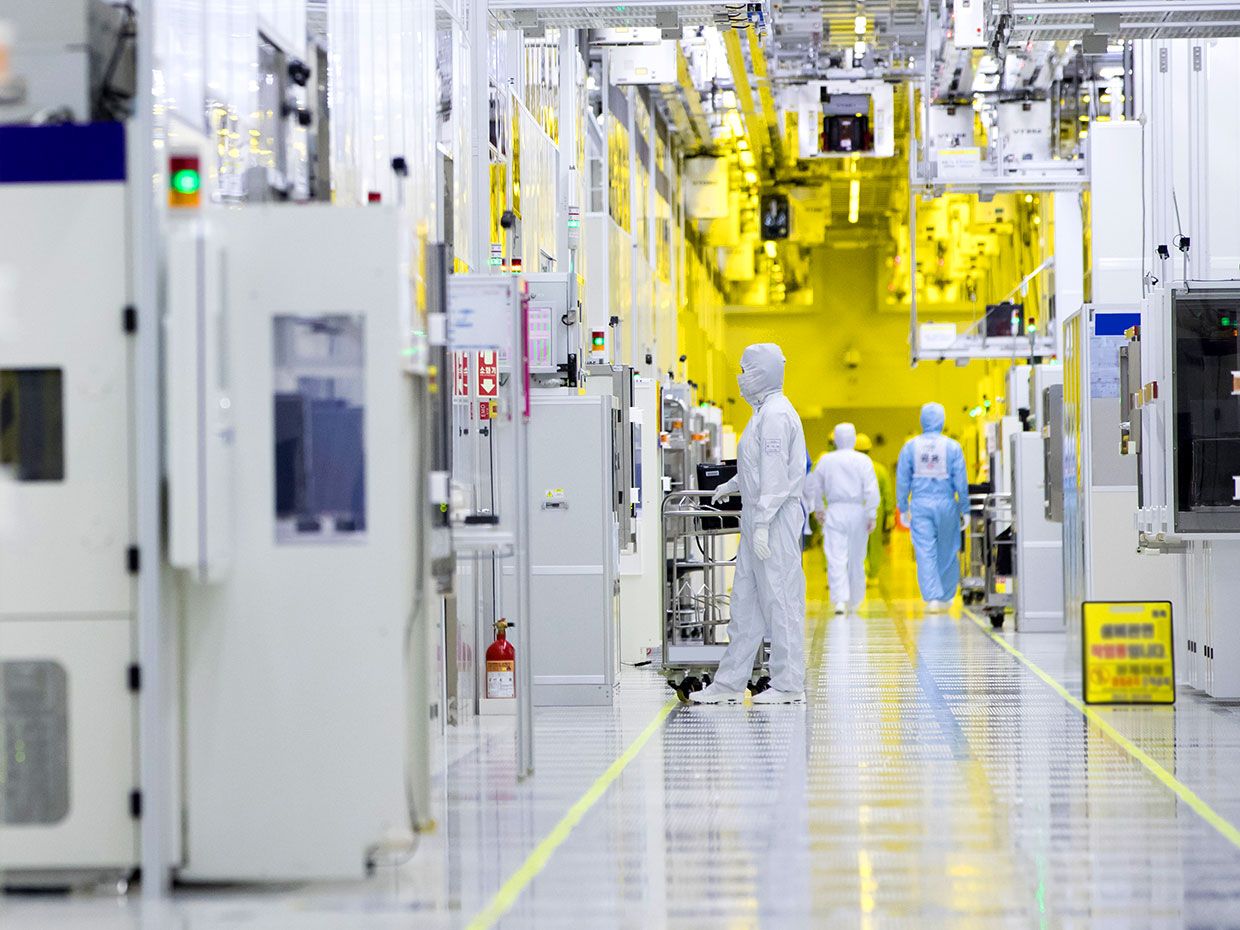
Two of the world’s largest foundries—Taiwan Semiconductor Manufacturing Co. (TSMC) and Samsung—announced in April that they’d climbed one more rung on the Moore’s Law ladder. TSMC spoke first, saying its 5-nanometer manufacturing process is now in what’s called “risk production”—the company believes it has finished the process, but initial customers are taking a chance that it will work for their designs. Samsung followed quickly with a similar announcement.
TSMC says its 5-nm process offers a 15 percent speed gain or a 30 percent improvement in power efficiency. Samsung is promising a 10 percent performance improvement or a 20 percent efficiency improvement. Analysts say these figures are in line with expectations. Compared, though, with the sometimes 50 percent improvements of a decade ago, it’s clear that Moore’s Law is not what it used to be. But judging by the investments big foundries are making, customers still think it’s worthwhile.
Why is 5 nanometers special?
The 5-nm node is the first to be built from the start using extreme ultraviolet lithography (EUV). With a wavelength of just 13.5 nm, EUV light can produce extremely fine patterns on silicon. Some of these patterns could be made with the previous generation of lithographic tools, but those tools would have to lay down three or four different patterns in succession to produce the same result that EUV manages in a single step.
Performance And Power-Consumption Improvements

Foundries began 7-nm manufacturing without EUV, but later used it to collapse the number of lithographic steps and improve yield. At 5 nm, the foundries are thought to be using 10 to 12 EUV steps, which would translate to 30 or more steps in the older technology, if it were even possible to use the older tech.
Because the photomasks that contain the patterns are so expensive and each lithography machine itself is a US $100 million–plus investment, “EUV costs more per layer,” says G. Dan Hutcheson, at VLSI Research. But it’s a net revenue gap on a per-wafer basis, and EUV will form the core of all future processes.
Who will use it?
The new manufacturing processes aren’t for everyone. At least not yet. But both companies identified some likely early adopters, including suppliers that make smartphone application processors and 5G infrastructure. “You have to have high volume and a need for either speed or power efficiency,” says Len Jelinek, a semiconductor-manufacturing analyst at IHS Markit.
Whom you’re competing against counts too, explains Kevin Krewell at TIRIAS Research. Graphics processing units, field-programmable gate arrays, and high-performance microprocessors used to be the first to take advantage of the bleeding edge of Moore’s Law. But with less competition in those markets, it’s the mobile processors that need the new tech to distinguish themselves, he says.
Is it okay that there are only two companies left?
Only Samsung and TSMC are offering 5-nm foundry services. GlobalFoundries gave up at 14 nm and Intel, which is years late with its rollout of an equivalent to competitors’ 7 nm, is thought to be pulling back on its foundry services, according to analysts.
Samsung and TSMC remain because they can afford the investment and expect a reasonable return. Samsung was the largest chipmaker by revenue in 2018, but its foundry business ranks fourth, with TSMC in the lead. TSMC’s capital expenditure was $10 billion in 2018. Samsung expects to nearly match that on a per-year basis until 2030.
Can the industry function with only two companies capable of the most advanced manufacturing processes? “It’s not a question of can it work?” says Hutcheson. “It has to work.”
“As long as we have at least two viable solutions, then the industry will be comfortable,” says Jelinek.
What’s next?
Chipmakers’ pipelines have traditionally had 5 nm following 7 nm and 3 nm following 5 nm. But analysts say to expect foundries to offer a variety of technologies with incremental improvements that fill in the gaps. Indeed, both Samsung and TSMC are offering what they’re calling a 6-nm process. Foundries will need those intermediate products to keep customers coming to the edge of Moore’s Law. After all, there aren’t many numbers left between 5 and 0.