According to Bloomberg Businessweek, spies in China managed to insert chips into computer systems that would allow external control of those systems. Specialized servers purchased by Amazon, Apple, and others around 2015 and manufactured in China by San Jose–based Super Micro were reportedly at issue, as may have been systems built for the U.S. military.
Amazon, Apple, the Chinese government, and Super Micro deny the incident ever happened. And some experts find it hard to believe a top-flight company like Apple could have initially missed something like this in their quality assurance process. However, other experts are convinced by Bloomberg’s reporting and the nature of the attack. One of those is Mark M. Tehranipoor, director of the Florida Institute for Cybersecurity Research (FICS). In fact, this is just the kind of attack his institute has been developing the technology to detect and counter.

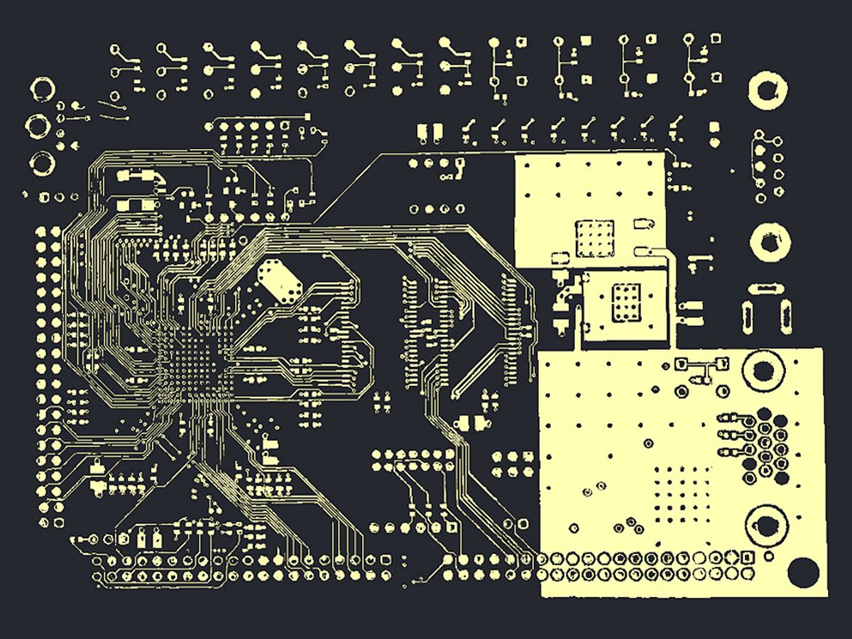
The institute’s semiautomated system “could have identified this part in a matter of seconds to minutes,” says Tehranipoor, an IEEE Fellow. The system uses optical scans, microscopy, X-ray tomography, and artificial intelligence to compare a printed circuit board and its chips and components with the intended design.
It starts by taking high-resolution images of the front and back side of the circuit board, he explains. Machine learning and AI algorithms go through the images, tracing the interconnects and identifying the components. Then an X-ray tomography imager goes deeper, revealing interconnects and components buried within the circuit board. (According to Bloomberg, later versions of the attack involved burying the offending chip instead of having it sit on the surface.) That process takes a series of 2D images and automatically stitches them together to produce a layer-by-layer analysis that maps the interconnects and the chips and components they connect. The systems in question in the Bloomberg story probably had a dozen layers, Tehranipoor estimates.
All this information is then compared to the original designs to determine if something has been added, subtracted, or altered by the manufacturer.
Nearly all of the process is automated, and Tehranipoor’s group is working on completely removing the need for a human in the system. In addition, they are working on ways to identify much more subtle attacks. For example, an attacker could potentially alter the physical values of capacitors and resistors on the board or subtly change the dimensions of interconnects, making them susceptible to system-crippling electromigration.
So why isn’t this system in widespread use? After all, much of it has been available since 2014. (Tehranipoor even described some in his 2017 article for IEEE Spectrum about the dangers of cloned chips.) “Sometimes a technology is ready, but it’s not used by companies because an attack hasn’t been seen to be real,” Tehranipoor says. This attack might be enough to change that perception, he says.
Even so, “this isn’t the attack that keeps me up at night,” says Tehranipoor. “As sophisticated as it was…those attackers could have done a lot more and been much more difficult to detect.”
Samuel K. Moore is the senior editor at IEEE Spectrum in charge of semiconductors coverage. An IEEE member, he has a bachelor's degree in biomedical engineering from Brown University and a master's degree in journalism from New York University.


