
In 1867, Jules Verne imagined spaceships propelled by the pressure of light. In 1871 James Clerk Maxwell predicted that such pressure actually existed, and in 1900 Pyotr Lebedev confirmed that prediction experimentally. But 109 years later, engineers have yet to find a practical use for this odd force.
Maybe it’s just too weak. Light pressure equals beam power divided by c, the speed of light. A one-milliwatt laser pointer, therefore, presses its object with the force of 3.3 piconewtons. You could lift a penny with laser pointers—you’d just need 30 billion of them.
Yet such weakness becomes a strength when you’re trying to nudge something of nanometer size and picogram mass. And the optics for directing light on such a scale already exist, in the form of miniature waveguides, couplers, and beam splitters, all of which are now routinely laid down on silicon-on-insulator substrates. We use these nanophotonic devices for optical processing. Why not also use them to exploit the ultralight touch that light itself can provide? Why not use light as an actuator, reaching right into the guts of an integrated circuit to throw tiny switches, either to control electronic circuits or, better yet, to reroute light itself, and the data that it carries?
Such a marriage of nanomechanics and nanophotonics would bring us a giant step closer to optical chips. That’s important, because light has a vastly wider bandwidth than electricity, which would enable it to get around the critical bottleneck in computing: the connections between processors. If light could act directly on circuit elements without first being converted to electricity, entire systems would run faster. You could imagine yoking together the multicore processors in a chip, making them run much faster and more efficiently than they can now. And if we really master the technology, optically controlled switches might ultimately supplant transistors, ushering in an era of all-optical computers. The resulting speedup would be stupendous, even by the standards of modern computing.
At the beginning of 2007, shortly after I joined the engineering faculty at Yale, I began to assemble a team to find ways of using light to drive silicon devices on a nanometer scale. We would be building on nearly two decades of research.
The quest had begun with microelectromechanical systems, or MEMS, which as the name implies are built in dimensions measured in micrometers. Today’s engineers find it easy to build resonators—tiny tuning forks, basically—at that scale by simply embedding them within electronic circuits. The circuits drive the resonators through electromechanical coupling, typically by pairing them with electrical plates—one fixed, the other on the movable MEMS. In such a scheme, a current applied between the plates alters the gap between the plates, which changes the capacitance and further induces a current that oscillates in response to the motion of the plates. Basically, you feed in a steady current and get an oscillating one in response. In a cellphone, for example, such oscillators are used in filters, picking out the desired signal from the swath of frequencies your antenna pulls in.
The smaller the size of the plates and the gap between them, the faster the oscillation can be and thus the higher the frequency that can be isolated. At the nanoscale, such oscillators attain the frequencies needed for microwave communications. However, the high frequencies give rise to complex impedances both mechanical and electrical. Because the structure is so small, the impedances are often badly mismatched.
How badly are they mismatched? In high-frequency circuitry you normally want every component to have an impedance of around 50 ohms. At these tiny dimensions, though, you’re going to end up with an impedance that’s millions of times as great, which means that essentially none of your signal will get through.
Scaling down from MEMS to nanoelectromechanical systems, or NEMS, also brings on other, more fundamental problems. First, in the nano realm, the oscillators are so fast that the conventional electronic circuitry they work with can’t keep up. Second, the oscillators’ signals are so faint that they can get drowned out by the random noise that’s endemic in any electronic circuit. A NEMS device can barely make itself heard over noise that’s just one-thousandth as strong as what you’d find in a typical IC.
Here is where photonics saves the day: Photons, unlike electrons, don’t interact with each other and so are immune to cross talk. Moreover, because light has a much greater bandwidth, or carrying capacity, photonic signals can carry far more bits per second than electronic signals, while dissipating much less power. Also, it’s easy to route photons on a chip; you just build a photonic wire—an optical nanofiber, essentially—on the top layer of the silicon in your chip. Finally, because we are in a purely optical domain, impedance is no problem.
The one big problem with those wonderfully noninteracting photons is that because they are noninteracting, there’s no obvious way to use one of them to control another. So that’s where the mechanical force of light comes in.
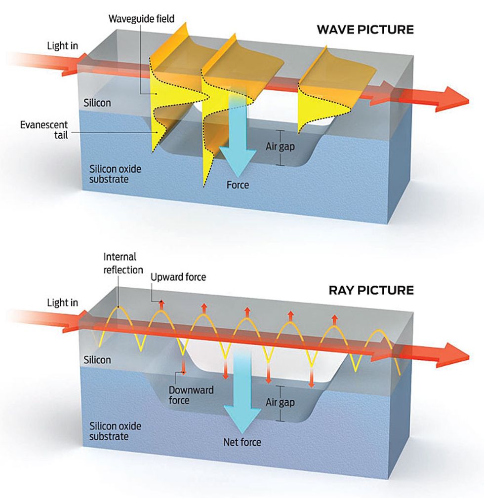
A Light Touch
There are two ways to picture the gradient optical force exerted in a waveguide. According to Maxwell’s equations [top illustration] the asymmetry between the open air on top of the waveguide and the thin air gap underneath will distort the optical field [yellow], creating a downward force.
Or you can resort to ray optics [bottom]. While in a conventional waveguide the light reflects equally strongly off the top and bottom edges, here the proximity of the silicon oxide substrate, with its relatively high refractive index, causes the rays to drag. They therefore push down harder than they push up.
Click on the image for a larger view.
One such force, of course, is straightforward radiation pressure, like that of sunlight pressing on the sail of a future interstellar spacecraft. However, you can’t harvest much momentum that way, and what you do collect will press in only one direction, which means you can’t use it to both push and pull things, an important consideration (as we’ll explain later). We therefore chose to exploit a different kind of optical force, one that often gets short shrift in university courses in optics. It’s called the gradient optical force, and it arises from an incredibly evanescent bonding between light waves [see illustration, "A Light Touch," above].
The gradient optical force was first used in the 1970s, in “optical tweezers,” which were designed to manipulate molecules in a kind of optical microscope. That such a force might also be used on a chip was suggested in 2005 by John Joannopolous’s group at MIT, together with Federico Capasso’s group at Harvard. Using theories ultimately derived from Maxwell’s equations, they concluded that it would be possible to generate a gradient force in the piconewtons, more than enough to get a nanometer-scale oscillator thrumming. The researchers based their calculations on a device involving two parallel waveguides, which are light-conducting channels engineered to confine waves of a given frequency in a beam so that it can travel through the guide with very little loss. Even though the two waveguides kept their beams separate, the bonding of the optical fields between the beams was surprisingly strong.
We found in 2007 that we could exploit the same principle to get oscillation using one waveguide rather than two. In the single-waveguide case, the optical field around the waveguide must be asymmetrical, in order to create the imbalance that’s needed to exert a net force.
Happily enough, you can create such a waveguide on a chip by etching away the oxide under a slab of silicon to form a slab, which looks rather like a tiny bridge. This slab can swing back and forth—that is, it can oscillate. Now when light propagates along the waveguide, it encounters asymmetry: The bottom boundary of the waveguide is separated from the silicon oxide substrate by a thin air gap—a dielectric substrate—whereas the top boundary borders on air alone. So, as Maxwell’s equations predict, a net optical force arises in the direction perpendicular to the waveguide. The force is substantial—well, for our purposes at least.
It may be easier to visualize the physics by means of ray optics. In a symmetric waveguide, the high refractive index in the middle guarantees that the light rays will bounce back and forth equally on the top and bottom surfaces of the guide. This perfect symmetry yields no net optical force. However, when a silicon substrate is present along the bottom of the waveguide, the rays are more strongly attracted toward the bottom surface, because the refractive index of the substrate—1.45—is higher than air’s 1.00. So think of it like this: The rays drag more forcibly along the bottom surface, applying a net force to the substrate.
So we’ve got ourselves a force and a mobile waveguide with which to harvest it. The next question is how to get light into the chip. It isn’t easy to generate photons in silicon, so they have to be fed to the silicon waveguide from an external laser, through standard optical fibers. That scheme turns out to be harder to carry out than it might seem.
Silicon waveguides are normally made just several hundred nanometers wide, so that at a wavelength of 1550 nanometers, a telecommunications standard, they’ll support only a single optical mode—a stable pattern that’s guided within the waveguide’s structure so that the signal doesn’t disperse. A standard optical fiber, however, is dozens of times as wide. When you hook such a waveguide to such a fiber, the modes won’t match up properly, and only about 0.1 percent of the light’s power transfers. It isn’t enough.
There are various tricks you can use to match the waveguide to the fiber, but because these tricks involve micromachining to an extremely high tolerance and at a very small scale, it is quite difficult. And the operations must be performed on each device, one at a time.
We found a better solution. In his lab at Caltech, Axel Scherer had developed some couplers for precisely this purpose: matching the light wave in an optical fiber to one in a silicon waveguide. Such couplers consist of optical gratings that are directly fabricated on silicon. Michael Hochberg, then a graduate student in Scherer’s lab, began collaborating with us in 2007 and walked us through the design of these couplers.
This grating coupler has a horn structure with openings at either end: a large one that connects to the optical fiber and another with a cross-sectional area just one-thousandth as big that connects to the waveguide. In this scheme, the fibers are aligned from the top of the wafer, and you can test hundreds of devices repeatedly. You can provide light on demand, piping it throughout the chip, bending, splitting, and recombining it at will. And because the coupler ensures that the light goes from the waveguide to whatever device it is driving on the chip, very little of the light leaks out because of diffraction.
Mechanical devices require proper anchoring so that they can oscillate for a long time without losing too much energy. However, you’d rather not have such an anchor in a photonic design because it would tend to disturb the guided light wave, causing photons to scatter and thus be lost. We had to come up with several approaches to overcome this problem.
First, we built an interface between the stationary waveguide and the mobile waveguide, providing rigid mechanical support and thus focusing the light waves. This structure is called a multimode interference coupler, and by working effectively as an in-plane lens, it keeps the loss of light below 1 decibel.
Next, we built a nanomechanical interferometer on a silicon chip. We wanted this device not only because its ability to detect motion very sensitively is inherently useful, but also because it would help us keep track of what’s going on in the various nanomechanical systems we devise.
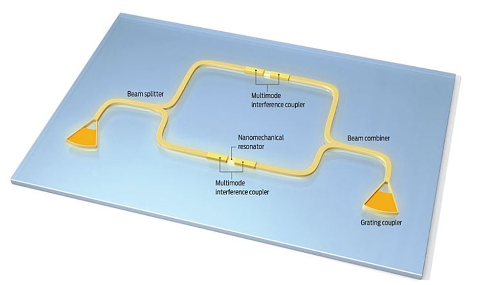
Motion Detector:
Photonic circuits form a chip-scale interferometer. Motion tends to modify the phases of the light waves, allowing an inference of the resonators’ oscillation.
Click on the image for a larger view.
We built a Mach-Zehnder interferometer, which splits one light beam evenly into two [see illustration, "Motion Detector," above]. One beam goes through a moving part of the device we’re building—say, the mobile, bridgelike part of the oscillator we described above. The other beam serves as the reference. A movement of the chip will cause the mobile part to vibrate, changing the effective refractive index through which the light is traveling and thus shifting its phase with respect to that of the reference beam. When the two beams recombine, their waves will interfere, forming a pattern from which we infer the degree of movement.
Our on-chip interferometer can measure movement to a sensitivity of 2 x 10¹⁴ meter, in a frequency range around 1 hertz. The spring constant of our devices—the measure of stiffness—is typically in the range of 1 to 10 newtons per meter. Therefore, the force sensitivity is on the order of 0.02 piconewtons, enough to resolve the gradient optical force—if it exists.
By the end of 2007 we had designed and redesigned the device—complete with interferometer, grating, and support coupler—many times. We were getting a reasonable amount of light through the measurement system, and almost all the components were in place. Yet even so, we still did not see the effect of the optical force. At this moment, our group suddenly received an infusion of new talent: Mo Li, a longtime friend and collaborator from my days as a graduate student at Caltech, where we’d both worked under Michael Roukes, a pioneer of nanoelectromechanical systems. We also welcomed Wolfram Pernice, a gifted photonic device designer who, after obtaining his Ph.D. from Oxford, joined us as a postdoctoral fellow.
By January 2008, Li had put together many complete chips with movable beams, but he could observe no evidence of the optical force in the vibration of those beams. It became a blind game. We couldn’t know whether the force was absent or simply undetected.
So we decided to separate the two problems of generating and detecting the optical force. To confirm that the interferometer was actually working, we actuated the device through the brute-force method of putting a sample chip on a piezoelectric disk, energizing the disk, and mechanically shaking the silicon photonic interferometer. The interferometer clearly indicated mechanical resonance.
Pernice worked around the clock and came up with new designs for the grating couplers and multimode interference couplers that allowed for much lower transmission losses, and therefore much greater sensitivity. Finally we were able to detect nanomechanical resonance at 10 megahertz without resorting to the piezodisk shaker. We therefore determined that the resonance had been induced purely by optical force.
The signal strength was enormous. With a slight increase of laser intensity, the beam resonance rose markedly, in nonlinear fashion. This result suggested that we could produce a force that was actually greater than we needed to move the picogram parts that make up a nanomachine. The actuation turned out to be just as efficient as that commonly used in MEMS devices, such as those that include inertial sensors of the kind used as gyroscopes. Of course, our NEMS system worked at a far higher frequency.
The next question involved the sign of the force. Just as electrically charged objects can either attract or repel each other, depending upon the sign of the charges, theory predicts that the gradient optical force should also be either attractive or repulsive, depending on the relative phase of the interacting light waves. Yet our devices exhibited only the attractive force. In other words, they were “monopolar.”
To create a bipolar device, we went back to the original MIT/Harvard theory, which considers the optical forces that come into play between two opposing waveguides. As two waveguides approach each other in parallel, that is, side to side, the theory predicts that the waves from each waveguide will overlap to form a bonding (symmetric) mode or an antibonding (asymmetric) mode. When the waves are in phase, the optical force is attractive; when they are out of phase, the force is repulsive.
To demonstrate these effects, we developed a butterfly-shaped circuit having two “wings.” In the left wing, the light is split equally into a top and a bottom arm, with the one on top having a longer waveguide to delay the light. This delay shifts the phase of the light waves. We then directed waves from each arm to recombine at the center of the butterfly, where the two suspended waveguides formed nanomechanical structures. If the light waves are out of phase at this point, the recombination should produce a repulsive effect. As for the identical right wing of the butterfly, its purpose is to make the whole structure symmetrical. That way, when the light proceeds into the right wing, the phase can be reversed, and the relative phase difference between both wings is maintained.
If the optical path difference between the two arms is an even multiple of the half wavelength, the waves will arrive at the nanomechanical devices in phase. The result should be an attractive force. If the delay is an odd multiple, you should get a repulsive force.
Everything worked according to theory. Better still, we found that by adjusting the relative phase of the interacting waveguide, we could tune the force from repulsive to attractive, or vice versa. (In practical experiments, we adjust the wavelength of the light source. This is equivalent to adjusting the delay phase in the wings.) In this fashion we have demonstrated all the predicted properties of the gradient optical force. Even more important, because this bipolar force can either push or pull, it allows us to manipulate components in both directions. We thus have complete control.
We achieved this push-me-pull-you control in late 2008. Now, instead of being limited to setting a vibrating beam in motion, we can push a nanomechanical lever in one direction—for instance, to open an optical switch and then pull it back again, closing the switch.
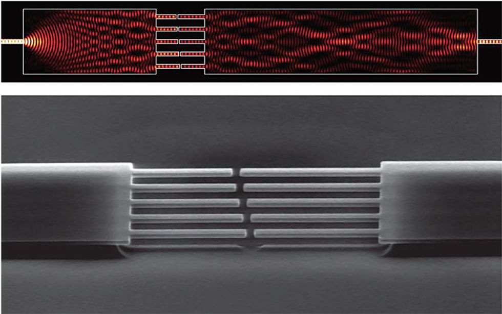
Harp Strings:
A single photonic bus feeds 10 nanoscale cantilever waveguides, each of a different length and thus vibrating at its own rate, like a harp string. Each cantilever can register a deflection of just a fraction of the diameter of an atom. Together they can measure complex patterns of motion.
Click on the image for a larger view.
The waveguide beams prove that optical force can be used to throw switches inside silicon optical circuits. Now we are extending that principle to other NEMS devices. Recently we embedded a series of cantilevers in photonic circuits, got all the cantilevers to resonate, and detected all their resonances at once [see illustration, "Harp Strings," above]. We did all this by sending a light beam via a waveguide, which branched off into subsidiary channels.
With this setup we can integrate many sensors on a single photonic bus. Such a design is fully compatible with the standard wafer-scale processes used to fabricate chips, so large arrays could be mass-produced in a straightforward and low-cost way.
The light-force interaction brings NEMS device development to a true circuit level, making possible all sorts of applications. Such a device would detect signals so faint that it could measure the weight of just a sprinkling of molecules on top of it. It truly would weigh the molecules, not just detect them, because it would measure the change in the frequency of the resonator.
Further out, we expect to use the nanomechanics and nanophotonics on a given chip to achieve dual-mode sensing—that is, an optical spectrometer and a resonant mass sensor. If you have a fluorescent molecule, you can use the spectrometer to determine what the molecule is by its color, and you can use the resonant mass sensor to tell how many molecules there are.
Of course, you could also use light pressure to process RF analog signals better than is possible today, by combining optical and mechanical filtering. Optical filtering can, for instance, let only microwaves through, whereas mechanical filtering—using the oscillating beams we discussed earlier—can filter at a lower frequency range.
We can imagine using optical force to reroute light on the fly, allowing a photonic circuit to perform at a blindingly fast speed, far beyond anything that electronic controls can manage. This capability would go a long way toward realizing the dream of an all-optical computer, able to exploit the immense bandwidth of light to its fullest. Maybe if you left your hard drive at home, you could read it at a comfortable rate over the Internet—if we’re still using hard drives by that time!
The most intractable bottleneck in today’s high-end computers comes from having to use electronic signals to control photons. The sky will be the limit when we can at last use light to steer light.
This article originally appeared in print as “May the Force of Light Be With You.”
About the Author
Hong X. Tang won a National Science Foundation Career award this year for using the pressure of light to operate nanomechanical devices. The award, worth US $400 000 over five years, is meant to encourage young scientists. Tang came to Yale in 2006 as an assistant professor of electrical and mechanical engineering.
To Probe Further
To learn more, go to https://www.eng.yale.edu/tanglab.