
The following is an excerpt from Multiphysics Simulation 2017.
By: Lexi Carver
In the 1980s, during the dawn of what would become a booming tech industry, flash memory made a splash by offering erasable and programmable computer storage. These storage chips now appear in cameras, memory cards, USB sticks, and phones that can store thousands of photo, music, and video files.
Though they often go unnoticed by consumers, designers work tirelessly to keep up with demands for smaller size and greater capacity. Behind the production of a single memory device stands a long line of researchers, engineers, and assemblers who must overcome the manufacturing challenges associated with processing these tiny chips.
KEEPING THE DIES INTACT
Memory chips are produced by placing a 300 mm diameter semiconductor wafer onto a carrier tape, then separating the wafer into single chips. Once removed, the tape leaves behind a thermoplastic adhesive on the chip undersides, later enabling bonding to a substrate using heat and compression. Chips are bonded into stacks to increase the amount of memory in a given area. Wire bonds connect the chips and the substrate. Finally, an entire sheet of stacks is put into a molding machine, encased in protective plastic, and then separated into many pieces, each containing a stack of memory chips (Figure 1).
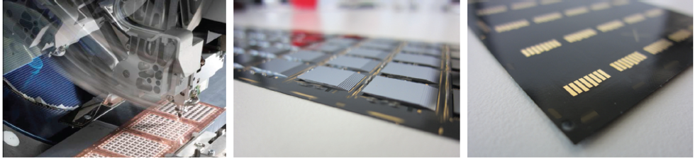 Figure 1. Top left: Dies being bonded onto a substrate before being wire bonded, coated in the plastic mold, and separated. Center: Stacks of dies on a substrate. Right: Back of the substrate showing the interfaces for connecting the memory chips to larger devices.
But removing the tape without bending the thin dies too much poses a tricky problem. With thicker chips from decades past, manufacturers used a multi-needle ejector to remove the tape using a series of pins. But these place too much stress on the thinner dies; the multi-needle ejector runs the risk of wrecking them.
“As chips got thinner eight or ten years ago, we were shocked at how many dies broke,” says Stefan Behler, senior expert process engineer at Besi Switzerland AG. “We needed a new way of peeling off the tape that wouldn’t bend the dies so much.” Besi develops equipment and assembly processes for substrate and wafer packaging production in markets such as consumer electronics, automotive, industrial, and solar energy.
After some brainstorming efforts, Behler and his colleagues landed on a new way to remove the tape using discs and vacuum forces that would be gentler than the multi-needle ejector. Their method consists of an array of parallel discs that lift up the microchip while the carrier tape is held flat by vacuum force. The discs move down starting at the outside, causing the tape to peel away from the microchip. The border between peeled and unpeeled areas underneath the microchip is called the “peel edge”. This edge moves inward, with a peel velocity dependent on the acting adhesive peel force (Figure 2).
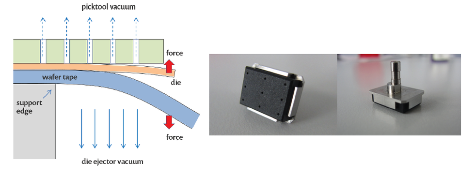 Figure 2. Left: Illustration of peeling used in the Multi Disc Ejector tool in the Die Bonder created at Besi. The pickup vacuum tool contains a rubber piece with holes for the vacuum pressure, shown at right.
One benefit of this method is that the propagation of the peel front is controlled by the moving discs, and the target die is only stressed along the peel front, Behler explains. Thus, the method is gentler than a multi-needle ejector, where the entire unpeeled chip area is stressed. “We had to make sure our system generates stress levels that are well below the strength of a given die,” he says. “If they bend too much during tape removal, they can crack or weaken.” They named their invention the Multi Disc Ejector and packaged it with the Die Bonder machine (Figure 3 and 4), which is now used by semiconductor packaging factories all over the world.
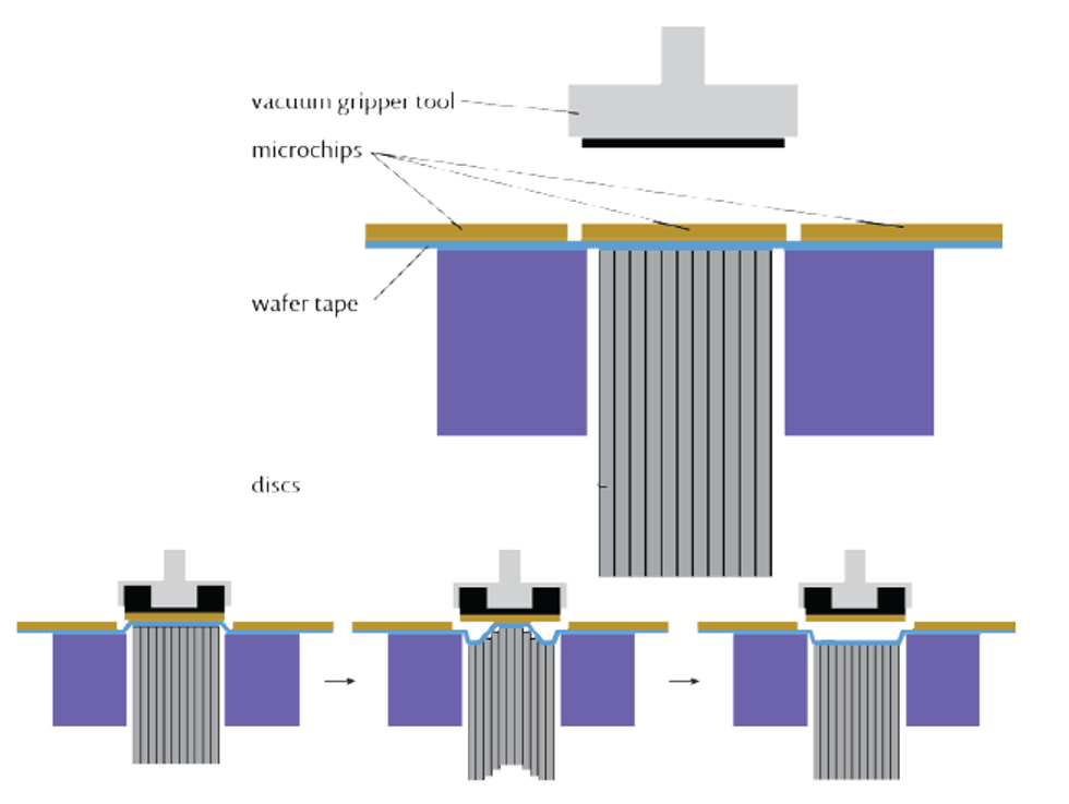 Figure 3. Top: layout of the Multi Disc Ejector. The bottom image shows a sequence of disc lowering over time during tape release while the pickup tool holds a microchip away from the tape.
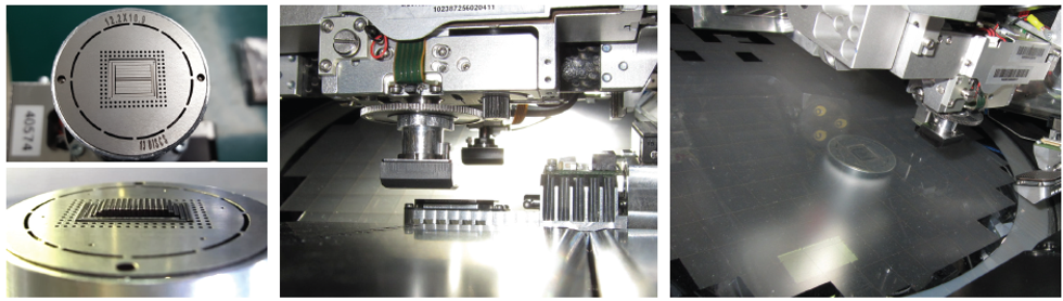 Figure 4. Left: Top and side views of the Multi Disc Ejector. Center: Pickup tool in the Die Bonder. Right: Tape removal in progress, showing empty wafer tape and the Multi Disc Ejector underneath.
SIMULATION TAKES US INSIDE THE EJECTOR
Once the design was chosen, selecting operating parameters for the Die Bonder required a deep understanding of the forces at play during peeling. “We wanted to know the maximum bending that would occur during the peeling process. This let us adjust parameters such as the disc height, speed, and vacuum force level, to make sure stress levels in the dies were low enough to prevent cracking,” Behler continues. To understand the physics, develop guidelines for ejector tool designers, and optimize the operating conditions, he used COMSOL Multiphysics® software.
Behler first built a static model (Figure 5) to test how the chip would bend under a certain disc geometry, vacuum pressure level, and initial peel length. Since he knew the stress level that would cause the tape to release from the die based on the material properties, he calculated the force in the vertical direction.
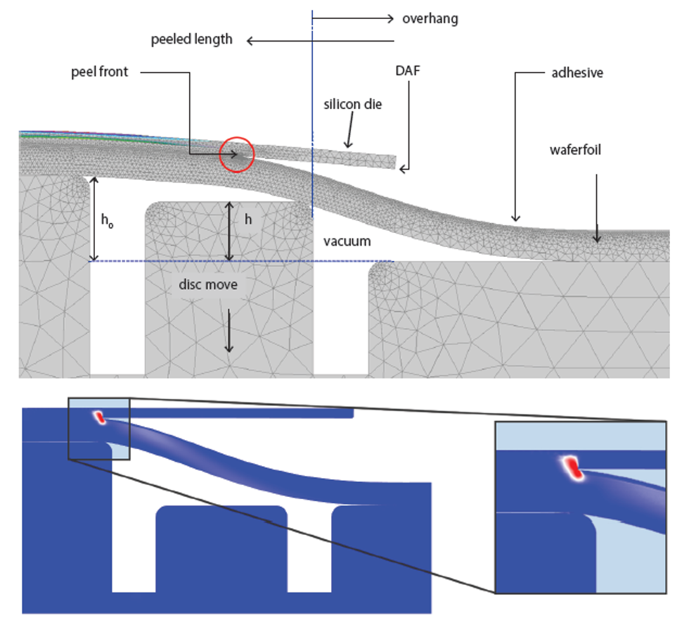 Figure 5. Top: Mesh of the geometry. Bottom: Simulation results showing stress in the vertical direction.
“I converted the stress results to find the peel energy or peel force, then compared this value to a data table to find the peeling speed,” Behler says. “I adapted the simulation to see how much the peel front propagated with each simulation step, to study how the chip bends over time. As the peel force and disc velocity increase, bending stress and likelihood of failure in the chip also increase.”
He calculated the maximum speed for the peel front’s propagation, which would determine the best speed for the discs (Figure 6) and thus the highest productivity achievable without breaking any dies.
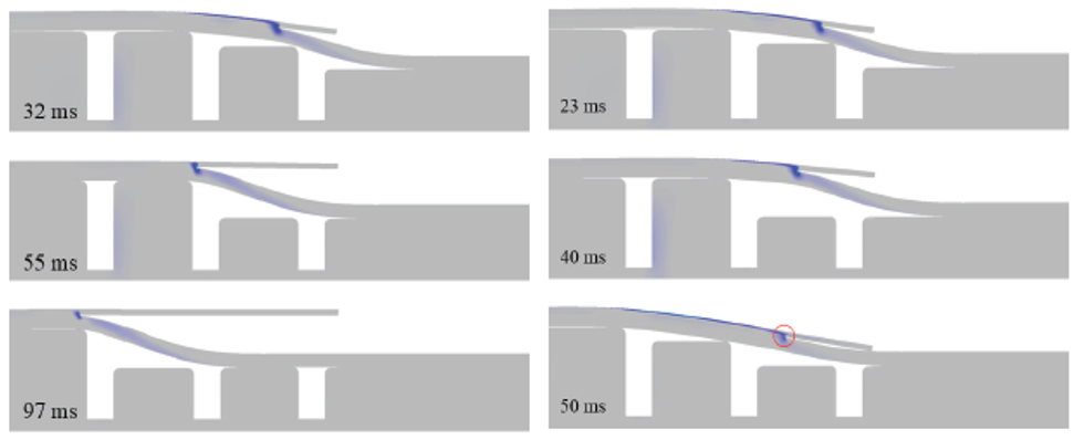 Figure 6. Simulation results showing stress levels for a peel front moving at 20 mm/s (left) and 32 mm/s (right). At 20 mm/s, the entire tape strip is able to peel free from the die/chip; at 32 mm/s, the die/chip becomes trapped and cannot be peeled: the red circle indicates how far the peel front has moved. It is not possible to peel any more by further disc moves, because the peel front is already too far away from the highest disc edge.
Behler also discovered that the animations he created with the software’s postprocessing features were helpful for visualizing what was really going on in the tape and die. “When you look at the machine, you can’t see what the ejector is doing,” he explains. “The animations actually helped people understand the dynamics of what was happening inside.”
ESTABLISHING CUSTOMER GUIDELINES
Following his modeling work, Behler was able to draw up guidelines for Besi’s customers using the Multi Disc Ejector. His team could now name specifics for Die Bonder operating parameters and chip setup, such as how far the memory chip can extend past the outermost disc for successful peeling. Since their customers use chips of many different sizes, they also manufactured different disc sets that can be swapped into the Die Bonder depending on the need. As memory chips continue to grow thinner and more powerful, Besi continues to lead the charge in computer storage packaging.
Click here to read the 2017 edition of Multiphysics Simulation and learn how mathematical modeling and multiphysics simulation are being leveraged as a powerful tool in many other industries.


