The Conversation (0)

ILLUSTRATIONS: STEVE STANKIEWICZ
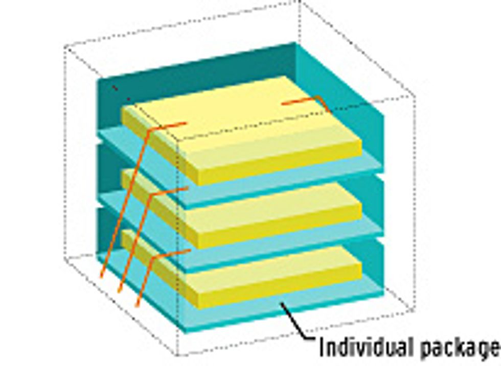
Stacked Packages
Packaged memory chips are commonly stacked on top of each other to supercharge memory in equipment ranging from cell phones up to high-end computers.
Packaged memory chips are commonly stacked on top of each other to supercharge memory in equipment ranging from cell phones up to high-end computers.
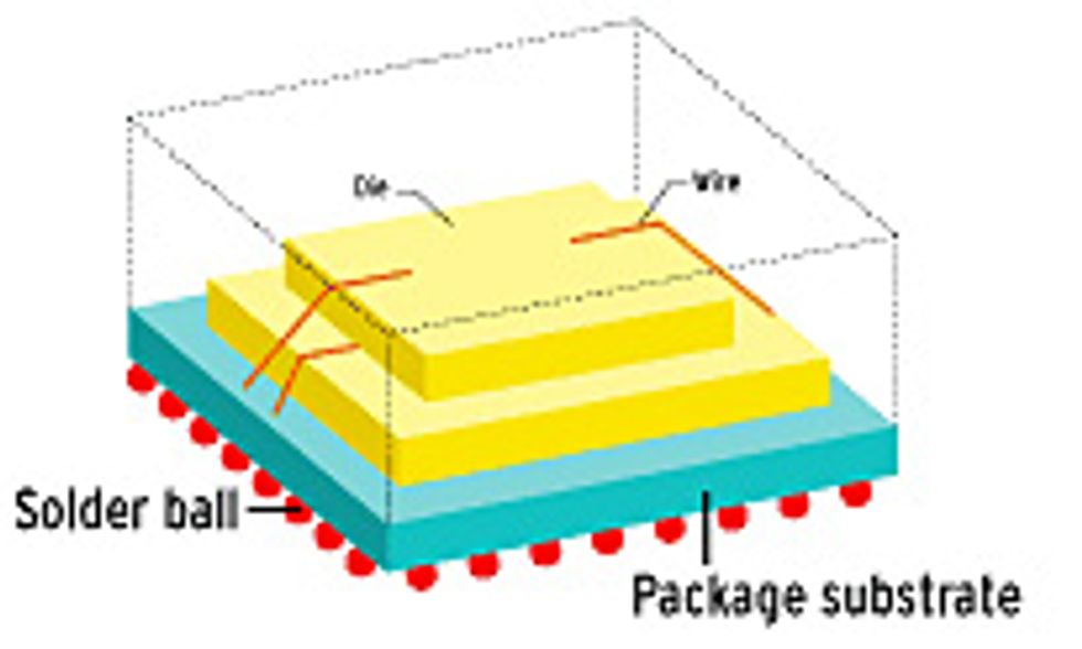
Stacked Chip-Scale Package
More compact are packages that stack bare die and wire-bond them to pads that connect to the solder balls leads on the substrate. The package is connected to a circuit board via the solder balls.
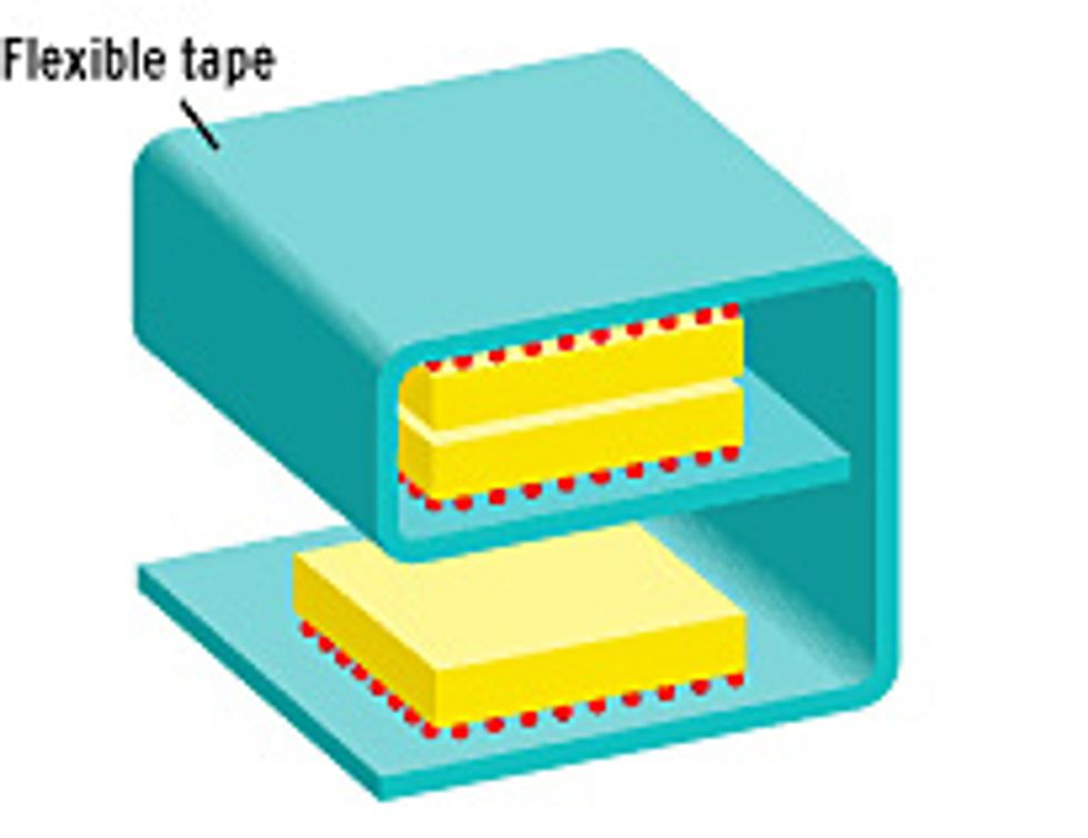
Folded Package
One of the newer ways for cramming capability into a small package starts with packaged chips on a flat polyimide tape. The flexible tape is then folded to yield a small footprint.
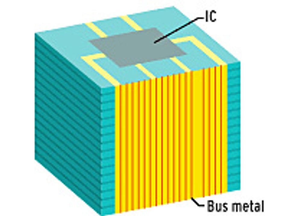
System-in-a-Cube
The densest package so far relies on a stack of epoxy layers in which are embedded different kinds of chips. Metal interconnects to the layers run along the sides of the stack.
Portable wireless communication devices, be they cell phones, personal digital assistants, or combinations of the two, are behind the drive to save yet more space on printed-circuit boards. In the last few years, a pair of two-dimensional approaches have emerged for combining processors, controllers, logic, and memory. One scheme designs all the components on a single silicon chip, while its rival squeezes two or more bare die into various kinds of multichip modules. It's system-on-a-chip (SoC) versus system-in-a-package (SiP).
So far, it hasn't been much of a contest. SoC unit shipments reached 345 million in 1999 and are projected to reach 1.3 billion in 2004, according to Cahners In-Stat Group, of Scottsdale, Ariz. The SiP market lags well behind: approximately 84 million SiPs were produced in 2000 and 770 million will be built in 2003, nearly two-thirds of which will go into wireless devices, according to Prismark Partners, of Cold Spring Harbor, N.Y.
But now, an evolutionary technology could put SiP into serious contention by exploiting the third dimension. Called system-in-a-stack, it crams more chips into the same board area by packaging the bare die in stacks [see illustrations]. Going upward instead of outward shortens interconnect distances, in turn reducing delays and capacitance and increasing speed and/or cutting power requirements. Shorter interconnects also reduce noise, further enhancing performance.
The idea of stacking chips is nothing new. Sharp Corp., Osaka, Japan, led the way in 1998, when it introduced the first stacked chip-scale package (S-CSP) of bare-die flash and SRAM for cell phones. Today Fujitsu, Hitachi, Mitsubishi, NEC, ASE, Toshiba, Dense-Pac Microsystems, and Amkor Technology are among the companies producing millions of different kinds of S-CSPs for portable communication devices.
In a typical package of this kind, two or three memory chips are piled on top of each other, separated by a thin layer of die-attach material and connected by wires to die-bond pads on the package substrate. Unit shipments of these packages reached 100 million in 2000, according to Jan Vardaman, president of the market research firm, TechSearch International, in Austin, Texas. She foresees that number doubling in 2001, with a growth rate of 20-30 percent per year expected for at least the next two years.
The advantages of stacking bare die are not lost on companies looking to go further and combine memory with digital signal processors (DSPs), application-specific integrated circuits (ASICs), and microprocessors. Intel Corp., Santa Clara, Calif., plans to start rolling out stacks of three and four memory chips in the next few months using a new technology from Tessera Technologies Inc., of San Jose, Calif., with which it could eventually achieve a system-in-a-stack by folding memory and logic together. Tessera pioneered chip-scale packaging in the mid-1990s with its patented microball grid array (µBGA), and now has a method for attaching memory chips, and soon ASICs, to flexible tape and folding the tape over to create low-profile stacks. Valtronic SA, of Les Charbonnières, Switzerland, already folds logic, memory, and passive components into a single package for hearing aids and other low-volume, high-value applications.
On the horizon is a system-in-a-cube based on epoxy-molded layers of different chips. Developed primarily for military and space applications by companies such as Irvine Sensors Corp., Costa Mesa, Calif., and 3-D Plus, Buc, France, these super stacks are now found in micro-cameras for satellites, and should make it possible to build more robust wearable computers.
The case for stacking
In early April 2001, an aggressive roadmap for 3-D stacked bare-chip packages was announced by Amkor Technology Inc., in West Chester, Pa. One of the world's largest contract manufacturers of semiconductor packages and test services, it was responding to increasing demand among customers for more system-in-a-package options. Amkor operates assembly plants in South Korea and the Philippines and plans to add 3-D packaging capabilities to new plants in China and Taiwan.
Amkor's 3-D stack offerings are a snapshot of the industry as a whole. The bare die are stacked in numerous combinations of wire bond, ball grid array, and flip-chip configurations. These combinations are very attractive to manufacturers like Motorola Inc., Schaumburg, Ill., that want to package an ASIC with off-the-shelf flash memory or DRAM, instead of embedding flash or DRAM in the ASIC itself.
"It's a fantastic way for companies to maximize their yields, by integrating die in the same footprint, but not in the same silicon," said Jon Woodyard, Amkor product manager for 3-D technologies. Such 3-D stacking also allows companies to offer a series of packages with the same dimensions but different functionalities. Depending on device types and the end market, a company could, for instance, combine a digital ASIC, an analog chip, a flash memory chip, and a DRAM chip in the same package in various arrangements of two-chip or three-chip stacks or, alternatively, with one or two chips laid out in 2-D next to a stack. This would save the costs of creating a different ASIC for each application.
Moreover, manufacturers can respond to competitive threats and add to their product line by simply stacking more die in the package. For example, a 16Mb flash memory could be added to a 32Mb memory package and it would all fit in the same 12-by-12-mm footprint. "They don't have to grow the package size now to make room," said Woodyard. "They just go vertical."
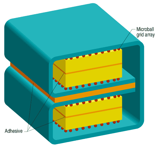
ILLUSTRATION: STEVE STANKIEWICZ
Four-Chip Stack Saves Board Space: Tessera's folded four-chip stack exploits chip-scale microball grid array (µBGA) processing to place die on a flexible polyimide tape. A special tool folds the chips twice, first to create two two-die stacks and then to fold the two stacks onto each other.
Click on the image for the full illustration view.
One technology Amkor is evaluating for inclusion in its suite of stacking solutions is the folded-stack technology from the aforementioned Tessera Technologies [see figure]. The company develops and licenses advanced packaging technology to the semiconductor industry and also provides design and prototyping services for chip-scale packaging. It is perhaps best known for the increasingly ubiquitous µBGA, a chip-scale package well suited to the folding process and indebted to its flexible and movable, or compliant, elements, for its excellent on-board reliability. The µBGA package has flexible S-shaped copper leads that connect the bare die to solder balls and ultimately the board. The encapsulant in the µBGA package is an elastomer, soft in comparison to the epoxies typically used for molding, explained Phil Damberg, the company's director of product engineering and pilot assembly. Together these allow the package to flex to absorb the strain caused by differences in the coefficients of thermal expansion between die and printed-circuit board or the flexible polyimide tape used in the folding process.
Folded stacks edge toward mainstream
Using its folded-stack technique and leveraging its µBGA technology, Tessera engineers collaborated with Intel for a year to mount three or four die in a package with a very low profile--less than 1 mm for a three-die stack, 1.2 mm for a four-die stack. Tessera said it can mount up to 14 die using the same method. With its customers already in possession of the manufacturing capability and licenses, Tessera is helping to move them to the folded-stack technology, first for memory applications and later for system-in-a-stack, starting with an ASIC, plus memory.
"It's an exciting technology for these companies," Tessera CEO Bruce McWilliams enthuses, "because they don't need to install new manufacturing lines to do stacking. They only add a tool at the end of the µBGA line to do the fold."
That sounds easier than it is. A four-die stack [again, see figure] starts out with a 40-mm-long rectangular strip of double-sided polyimide tape (Kapton or Upilex), 25 or 50 µm thick. Each side of the polyimide tape has a metal layer that holds all the leads and interconnects between the chips, similar to a printed-circuit board. Chips of flash, SRAM, or DRAM go through standard µBGA processing. The die are affixed to the tape with either silicone- or epoxy-based die-attach material and are lead-bonded and encapsulated. Solder balls are then attached to the pads on the tape on what will be the bottom portion of the package. At the end of the line, instead of punching out finished single µBGA packages, the strip of four chips is forwarded to the two-step folding process.
This starts with a silicone adhesive being dispensed on the backs of the middle two die. The outer two die are folded on top of the middle two by a special tool to create a pair of two-die stacks. More adhesive is dispensed onto the two stacks, which are then folded onto each other. The tool shuttles the folded stack into a fixture that holds the package together while the adhesive cures. The finished module is mounted on its circuit board by means of the solder balls put on the flex tape earlier.
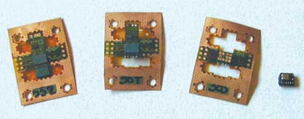
IMAGE: VALTRONIC
Folded Hearing Aid Includes Passive Devices: Valtronic folds passive and active components in the same package. This hearing aid module has flip-chips mounted on one side of a polyimide film substrate and passive components surface-mounted on the other. The bottom portion is folded up, the top folded down so the flip-chips are folded inside and the passive components are on the outside. The complete module [far right] is then cut free.
According to Ted Tessier, Amkor vice president for advanced application development, Tessera's folding technique yields the lowest possible package profile. The reason is that die of the same size are stacked without the silicon or film spacers required to separate the chips inside stacked chip-scale packages. Like all chip-scale packages, the folded-stack solution will have only slightly bigger planar dimensions than the largest die in the stack.
Another advantage of flex tape compared to certain conventional S-CSPs is routing density. S-CSPs connected by ball grid arrays to rigid FR-4 (fire-retardant epoxy resin/glass cloth laminate) package substrates are generally limited to 40-µm lines and spaces. That's because these substrates derive from printed-circuit board manufacturing processes, which favor large panel formats and are limited in lithographic resolution and etch processing. In contrast, the minimum lines and spaces on flex tape are 25 µm. Because the routing density for tape is better than for ball grid array S-CSPs, a folded-on-flex package will permit a smaller overall package footprint.
Despite these advantages, Amkor is holding off adopting the technology until a number of technical and supply chain issues are resolved. One of these is the availability and cost of the double-sided polyimide tape.
The high cost of the double-sided versus single-sided tape is due in part to the additional process steps and different manufacturing lines it involves. Damberg says that Tessera has been working with high-volume substrate suppliers to get costs down. Ultimately, the price will depend on how many high-volume customers opt, like Intel, for the folded-stack design. Tessera is also telling customers that cheaper single-sided tape will suffice for certain folded-stack applications.
Getting the heat out
Then there's the heat extraction problem that 3-D packages in particular face. In a three-die stack, the bottom chip nearest the circuit board dissipates heat efficiently, while the top and especially the middle chip in a stack, don't. One partial solution is to put the high-power-dissipation die at the bottom of the stack because 85-90 percent of the total amount of heat dissipates through the mounting board.
This isn't as much of a problem as it seems for memory applications because power dissipation levels are not high. While flash memory chips consume anywhere from 0.15 W to 0.4 W each, Young-Gon Kim, director of product design and reliability for Tessera, points out that under real operating conditions, "all devices are not in active mode. Many of them dissipate less heat in stand-by mode. So the overall power dissipation of a stacked package is much lower than the number of die might suggest."
Tessera engineers know, though, that they have to come up with more aggressive heat dissipation strategies to accommodate higher-power ASICs, which often dissipate 10 W or more. Consequently, the company is exploring ways to optimize the thermal performance of the package by tweaking its structure and employing various combinations of high-thermal-conductivity encapsulant, copper ground plates, and heat-spreaders.
While Intel and other Tessera customers plan to roll out folded-stack packages of memory in the next few months, Valtronic, the Swiss company mentioned earlier, has been folding logic, memory, and passive components together into packages for the last two years. Although Valtronic's packages are the taller, Tessera's have thus far managed to include only memory, not logic, and certainly not passive components.
Valtronic, a US $50-million-per-year contract manufacturer, provides custom-designed folded system-in-stacks in relatively low volume to customers producing under one million units per year. For example, it used its patented 3D Chip Scale Package (3D-CSP) technology to fit the world's smallest hearing aid in a module measuring 4.5 by 4.0 by 3.0 mm and incorporating a central processor, a digital signal processor, an EEPROM chip, and 18 passive components.
ILLUSTRATIONS: STEVE STANKIEWICZ
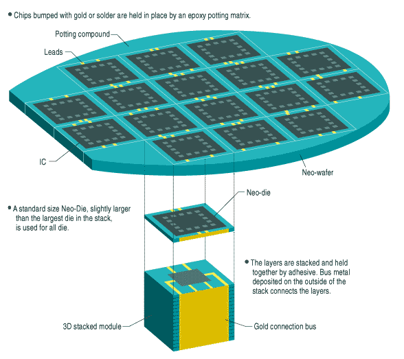
Die Stacks Can Be Mass Produced: In Irvine Sensors’ Neo-Stack process, chips for layering are embedded side by side in an epoxy matrix shaped like a silicon wafer, which permits the use of standard assembly-line equipment. The layers are sliced out of the epoxy wafer and stacked into a module. Bus metal is deposited on the outside of the stack to bring the I/O from the chips to the cap chip.
Click on the image to enlarge.
Silicon burrito
In the folded-stack scheme that Valtronic uses for high-reliability products, such as heart defibrillators and hearing aids, gold is key. Gold stud-bump flip-chips eliminate die-bond wires, reducing circuit wiring lengths and minimizing most of the interconnection's resistance, capacitance, and inductance, and can typically accommodate over 500 connections per die.
Valtronic starts with double-sided flexible polyimide strips 25-50 µm thick. Like Tessera, Valtronic sometimes uses Kapton, but also uses other kinds of polyimide strips, whose composition the company would not divulge. Gold pads are deposited on the tape, covered with a nonconductive, non-silicone-based adhesive, and have flip-chips stud-bumped with gold pressed down on them. The adhesive minimizes thermal expansion effects between the die and the tape, so that when the polyimide tape heats up and moves relative to the silicon chip, the gold bumps and pads also move, but never lose contact. The fatigue and stress associated with solder joints used in other flip-chip processes are altogether absent.
While gold contacts provide the kind of high reliability required in medical implants, there is a size limitation on the stud-bumped flip-chips used by Valtronic, which can at best accommodate a 110-mm bond pad pitch. In contrast, Tessera's µBGA package can accommodate an 80-mm bond pad pitch for perimeter bond pads, allowing the company's customers to use smaller chips.
After the flip-chips are attached to the flexible tape, passive components are surface mounted to the bottom side. Components differing in both type and size, from flat die measuring up to 2 mm2 to cube-shaped resistors and capacitors measuring up to I cm3, can be mounted within I mm of each other. To some extent, the passive components, being bulkier than the active components, end up dictating the size of the package.
For the kind of three-layer folded stack used to create the hearing aid module, the unfolded packages start out on the strip in a cross configuration and are wrapped up like burritos. First, the bottom portion of the cross is sliced free from a reel of tape by a laser and folded toward the middle, after which the top portion is sliced and folded down. A laser then cuts the module free from the strip, and potting material is flowed into the center of the package [see photo].
Unlike Tessera's rectangular tape strips, Valtronic's layouts can vary. Even L-shape and S-shape strips are possible, so that the manufacturing process resembles high-tech origami. The shape depends on the application. Gary Pinkerton, director of sales and marketing for Valtronic USA Inc., explained: "Typically, the final package volume requirements and the size of the components drive the layout. At other times, components must be isolated from other components, so we place them as far away as possible."
The Swiss company's miniaturization doesn't come cheap. But its clients are willing to pay for minimal inductance and capacitance, which after all translates into the lower power consumption and longer battery life especially important in medical implants.
System-in-a-cube
As stacking technology begins to enter the mainstream, companies like Irvine Sensors Corp. are already several generations ahead of the competition, having developed a technology for military and space customers that stacks tens of layers of different chips together. Rather than folding a strip of tape with parts attached, Irvine Sensors embeds groups of chips in an epoxy matrix shaped like an ordinary round silicon wafer [see top part of figure]. This matrix can then be processed with standard wafer tooling and fixtures to produce a system-in-a-cube that Irvine Sensors markets under the Neo-Stack trademark. Four Neo-Stacks ganged together could, for example, give wearable computers the power of a workstation in something the size of a deck of cards. Irvine Sensors is beginning to see interest in system-in-a-cube embedded applications from the industrial community, for which it expects to begin initial production in 12-18 months.
Irvine Sensors' Neo-Stack starts with known good die (KGD), nonpackaged ICs that have gone through burn-in and testing similar to packaged ICs to ensure a high yield of finished modules. KGD are expensive compared to untested die, and are often eschewed by companies that can tolerate the loss of a few bad, but cheap, modules such as stacks of flash or SRAM. But for the complex stacks of different chips in which Irvine Sensors specializes, KGD are vital.
The first step in the Neo-Stack process is to take the KGD and bump the I/O pads with gold or solder. The chips are then grouped together into what will become individual stack layers, each slightly larger than the largest die in the stack. Every layer is a standard size, although each individually may have different chips.
"Neo-Stacking allows us to mix and match practically any type of component, be it optical, microelectromechanical, electronic, or optoelectronic in a stacked package," said Volkan Ozguz, manager of technology R&D for Irvine Sensors.
As the chips are bumped with gold or solder, photosensitive polyimide film is spun onto a thin piece of aluminum, called a shim, that aligns the film. A mask made to match the bump locations and the dimensions of the chips to be embedded is laid over the polyimide film. After the film is exposed, the shim-film assembly is bonded to a glass-epoxy-based carrier, the shim etched away, and the bumped chips embedded on top of the polyimide film. Potting epoxy fills the cavities and the Neo-wafer is cured.
Next, the wafer is lapped, exposing the planar surface of the polyimide with the flattened bumps flush with the surface. Metal traces are deposited to bring I/Os from each layer to two sides of the stack. Metal interconnects among chips on the same layer are deposited and then covered with a protective layer of polyimide. Using a mask, vias corresponding to the location of the bumped pads on other layers can be added to create a multilayer interconnection structure.
The Neo-wafer is then ground on the bottom to the desired thickness of 150-200 µm and diced into individual layers, which are stacked according to the package design and are held together by a 1-µm-thick coating of adhesive [see bottom part of figure opposite]. The stack is capped with a polyimide glass substrate, which is coated with metal on both sides and connects to the rest of the stack through vias. The stack sides are then lapped to expose the interconnects. At that point, bus metal is added to two sides to complete the interconnects between the layers and bring all the I/O signals to a cap chip on the top [not shown in figure ].
Using this technology, Irvine Sensors has fashioned Neo-Stacks with up to 48 layers. Ozguz points out that there are no fundamental limits on how many layers the Neo-Stack can accommodate.
Epoxy resin does not dissipate heat as efficiently as silicon. So to improve heat transfer between layers, blank pieces of silicon are sometimes added to open areas on layers where smaller die are used. Thermal sinks, such as copper plates that shunt heat to the sides of the stack, can also be added to provide lower thermal resistance. Advanced techniques of this kind allow Irvine Sensors to create stacks that handle 50-60 W--at least an order of magnitude higher than most of today's 3-D packages, according to the company.
Ensuring good yields
Testing and yields have been major stumbling blocks for stackers for one simple reason: if there's one bad chip in a stack, either it must be replaced or the whole package discarded. This is less of an issue when commodity memory is being stacked, but is a serious concern when more expensive ASICs or CPUs are being thrown out.
To combat the problem, Valtronic runs tests in the prototype stage after each flip-chip is applied, and conducts a functional test after the passive components are added. Full functional verification is performed again after folding. Once production is in full swing, however, a functional test is performed on the completed module only. Because the Neo-Stack starts out with known good die, yields are expected to be very high. Also, each layer of the Neo-Stack is tested individually after it's diced. In some cases, redundant components are provided within the stack to further lower risk of failure.
Compared to currently available two- and three-layer stacks, the Neo-Stack modules come at a premium. Then again, reliability, not cost, is the critical issue for Irvine Sensors' performance-driven military and space customers. They include the Defense Advanced Research Projects Agency, Ballistic Missile Defense Organization, and NASA, for whom the company variously developed the system-in-a-cube technology for use in wearable computers and satellite applications.
For government vendors, the wait for the commercial sector to grow into advanced technologies initially developed for military and space applications is irksome, to say the least. But Ozguz is confident that the trend toward system-in-a-stack will continue its upward trajectory toward ever more complex applications. "Competitors such as Amkor, Tessera, and Sharp, which are offering two- or three-layer stacking, are helping to convince mainstream application designers that 3-D stacking is a viable approach," Ozguz said. And when customers are ready to move up to the next generation of system-in-a-stack solutions, Irvine Sensors will be ready to oblige.
Harry Goldstein, Editor
To Probe Further
A more up-to-date exploration of 3-D packaging is "The Advent of 3-D Package Age" by Larry Wu and others. The paper appeared in the Proceedings of the 2000 IEEE/CPMT International Electronics Manufacturing Technology Symposium, pp. 102-07.


