Thin-film transistors (TFT) form the foundation for many of today’s technologies, including smartphones and flat-panel TVs. And these TFTs are made possible by amorphous silicon. While this material has managed to do the trick for the most part, it does have some performance limitations, such as limited carrier mobility, that have sent researchers in search of something better.
Organic thin-film transistors (OTFTs) have proven better than amorphous silicon-based TFTs in some areas of performance, especially carrier mobility. Unfortunately OTFTs have their own problems—in the critical performance parameter of large threshold voltage instabilities, they are poor performers. Threshold voltages—also known as gate voltages—are the minimum voltage differential needed between a gate and the source to create a conducting path between the source and drain terminals.
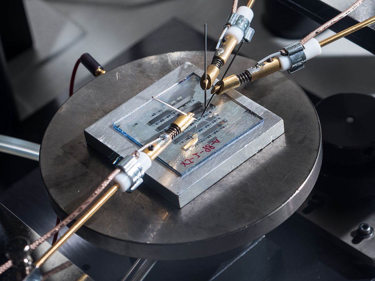
Now, researchers at Georgia Institute of Technology have developed a nanostructured gate dielectric that overcomes this obstacle of voltage threshold instabilities in OTFTs, and could lead to wider use of organic semiconductors for thin-film transistors.
A gate dielectric is a key part of every thin-film transistor. It is the electrically insulating layer between the gate electrode and the semiconductor. It should have a high dielectric constant, be very thin, and have a high dielectric strength for the transistor to operate at low voltage.

When a voltage is applied to the gate electrode, the resulting electric field across this insulating layer modulates the density of carriers in the semiconductor layer and controls the current that is flowing between the source and drain electrodes. Chip designers choose from many different materials to form this insulating layer, from single dielectric polymers, to inorganic oxides, to combinations of different organic and inorganic materials.
In research published in the journal Science Advances, the Georgia Tech researchers used atomic layer deposition (ALD) to grow a thin metal oxide layer on top of a perfluorinated dielectric polymer.
They chose atomic layer deposition for its ability to produce layers that are free of defects. “The low defect density reduces the diffusion of moisture into the underlying organic semiconductor layer, preventing its degradation,” said Bernard Kippelen, a professor at Georgia Tech, and leader of the research.
Kippelen notes that ALD was initially developed for traditional CMOS-based technology, but that his research group pioneered its use in organic thin-film transistors.
Initially, the geometry of the gate dielectric was comprised of a perfluorinated polymer layer and alumina grown by ALD. However, under high relative humidity conditions, alumina degrades through corrosion.

“In this work we replaced the alumina layer with a nanolaminate that consists of alternating nanometer-thick layers of alumina and hafnium oxide,” said Kippelen. The nanolainates were less prone to degradation.
The performance of the new organic thin-film transistors appears to exceed that of hydrogenated amorphous silicon technology, both in terms of charge mobility and stability, according to Kippelen.
Kippelen concedes that the charge mobility achieved with the version used in their studies is inferior to that of the best metal oxide semiconductors. However, he argues that new organic materials already exist that yield higher mobility, and which simply need to be tested in the new geometry.
“It is premature and difficult at this stage to provide a direct comparison with what is currently on the market; nevertheless, we believe that the level of stability that is achieved is an important step for printed electronics,” he said.
With this step, Kippelen and his team envision that these advances could make it possible to manufacture large-area products such as displays.
Of course, Kippelen notes that additional engineering must be carried out to address scaling and throughput if these devices are to be used in commercial electronics. But he believes as conventional ALD is replaced with a next-generation ALD that utilizes multiple heads with nozzles to deliver the precursors much faster, combined with direct-write inkjet printing for the other layers, there exists a clear path for devices to be scaled up in size with large throughput.
Before that future is realized, Kippelen and his team will further investigate the mechanical properties of these printed transistors since they are likely to be used in large-area products with flexible form factors. They will also continue to investigate the fundamental mechanisms behind some of the compensation effects they have observed in these devices to gain a better understanding of their operation.
Dexter Johnson is a contributing editor at IEEE Spectrum, with a focus on nanotechnology.


