A few years back, I noted that the concept of materials by design had fallen out of the lexicon of nanotechnology proponents and suggested that this was due, at least in part, to how difficult it would be to achieve.
I received some pointed criticism for my view, which was characterized as being so conservative as to be radical.
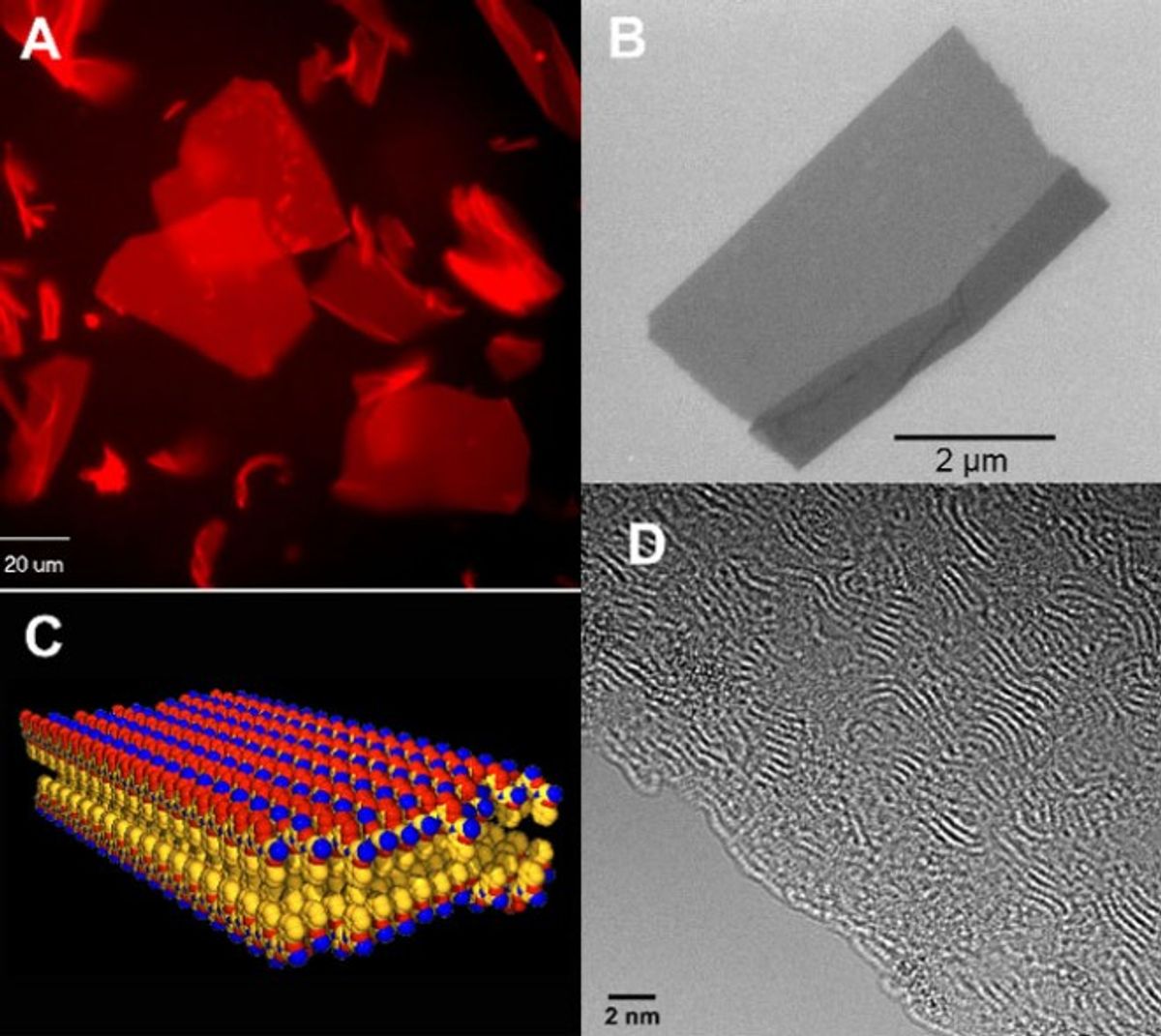
When I saw recent news that researcher Ronald Zuckermann and his colleagues at Lawrence Berkeley National Laboratory had manufactured a large sheet, just two molecules thick, made of a polymer that mimics the precise structures seen in proteins and crystal structures, this “material by design” debate occurred to me once again.
While this possibility hints at the potential of material by design, earlier in the article the more accurate description of how this material came to be designed indicates that it followed a far more an iterative process than a deliberate one: “Zuckermann’s team made the discovery by stumbling upon a particular sequence of repeating units that formed perfectly aligned two-dimensional crystals.” (Emphasis added).
This question of material by design aside, the perfectly aligned two-dimensional crystals made into such a large structure is a remarkable achievement. It has been described as the “plywood” for building the electronic devices of the future.
Suggested applications are numerous ranging from tissue engineering and drug delivery to batteries and fuel cells. Clearly applications in which flat electrical components are needed such as in photovoltaics are a likely area for initial applied research.
Dexter Johnson is a contributing editor at IEEE Spectrum, with a focus on nanotechnology.


