16 September 2009—Dissecting tiny semiconductor chips and guessing how they're made sounds like a hobbyist project, but it's a bona fide living for the reverse-engineering firm Chipworks, based in Ottawa, Ontario. Dick James and other Chipworks engineers like to sniff out what's going on beneath the surface of chips, using their knowledge of the industry combined with some sophisticated chemical analysis.
What they're finding now are a deluge of "dummy features"—structures that don't improve the performance of the chips at all but rather yield more functional and reliable chips on each silicon wafer.
Dummy features are the most visible manifestation of a trend called design for manufacturability, or DFM, and it can mean using different materials, designing new layouts, or adopting specific processes to increase reliability and yield. "DFM features have no functionality on the chip but make the process more uniform, more reproducible, more manufacturable," James says. "We've started to see more and more [dummy features on cutting-edge chips]" [see sidebar, "How Dummy Features Are Found"]. James presented the latest examples of DFM this week at the IEEE Custom Integrated Circuits Conference.
Manufacturers use dummy features to even out the strain on the chip's transistors and to enhance the lithography process, among other things.
As feature sizes have shrunk to below 90 nanometers, chipmakers have strained the bonds between the silicon atoms to increase transistor performance. A "stress layer" such as silicon nitride is stretched over the transistors, improving the conductivity through them. However, uneven strain over the features makes for less noticeable improvement. Hence, says James, you need to even out the strain, which you can accomplish with dummy features.
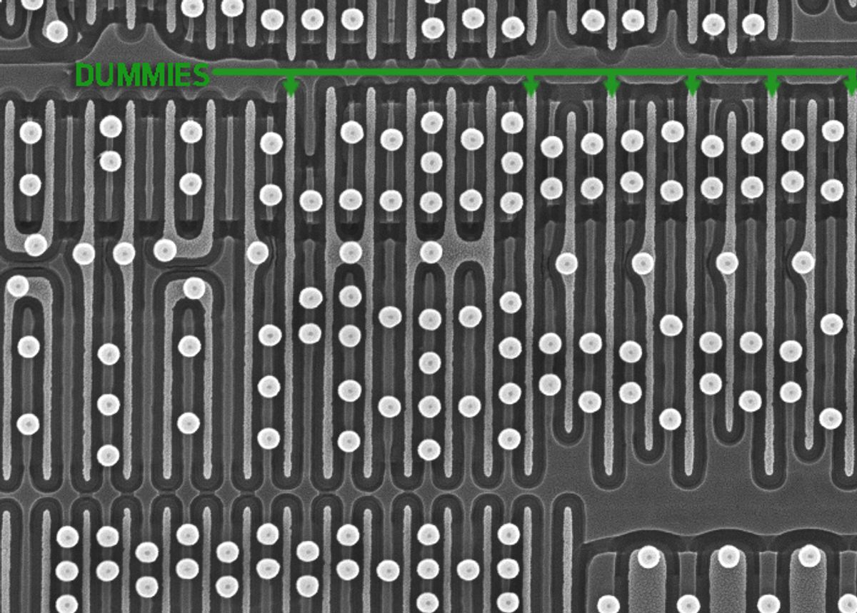
When engineers at Chipworks took apart Advanced Micro Devices' 65-nm Athlon chip, they found lines of transistor gates arrayed vertically and spaced evenly over the chip (the circles in the photo are tungsten metal contacts). But not all the lines are part of the circuit. AMD squeezed in lines of dummy polycrystalline silicon, or polysilicon, to keep the pattern uniform, which in turn evens out the applied stress across the gates.
AMD Athlon
Dummy features also aid in optical lithography, a chipmaking technique in which a circuit's pattern is projected onto the silicon using laser light. Optical lithography is reaching its limits as circuit features get much smaller than the wavelengths of light used to pattern them. Companies can't just get away with tweaking the lithography process itself anymore, James says. "Instead, you have to design the chip features to compensate," with manufacturability in mind.
So when Chipworks examined the innards of one of Texas Instruments' 65-nm systems-on-a-chip, they found lines of dummy polysilicon that were most likely added for lithography purposes, to shape the light pattern a certain way. The lines were spaced too far away from the active silicon [rectangles] and polysilicon gates [vertical lines] to be practical for stress relief.
Texas Instruments SoC
Intel, too, has "gone gung-ho for dummy features," says James, incorporating advanced illumination and double-patterning lithography techniques that show clear design with manufacturing in mind.
Intel Xeon
James says that features in the 45-nm Xeon chip suggest that Intel improved the resolution of its lithography with a technique called dipole illumination, a process that splits light into two beams, sends them through reduction lenses, and projects features from different angles. This process works best when illuminating parallel lines, the likely reason for the dense, all-parallel structures, James suggests, including the row of dummy gates that add to the density and uniformity of the design. The Intel layout, according to James, demonstrates how chip features and manufacturing processes have to be designed together—not one after the other—to maximize performance and yield.
James also believes the Intel process was done with dry lithography, which makes it the only chip at 45 nm to do so. (The alternative is "wet" or "immersion" lithography, which requires machines that are more expensive.) And the Intel 45-nm chip uses gate stacks made of metal and high-k dielectrics instead of polysilicon and silicon dioxide, thereby reducing leakage in the transistors.
Intel is "pushing the envelope with [these] design technologies...with impressive results in yield as well as processing uniformity," says James.
Not everyone is so invested in DFM, however. A 65-nm field-programmable gate array, or FPGA, designed by Xilinx and Toshiba uses no dummy features and flaunts conspicuously unclaimed silicon real estate. The designers could squeeze transistors closer together to save area at the transistor level, James says, but they'd most likely have to change the interconnect layer and any number of other parts to do so. "You change one thing, and you have to change half a dozen other things" to compensate, he says.
Xilinx and Toshiba FPGA
It's a calculated trade-off: the cost of silicon versus the cost of more-complex masks and manufacturing. Sometimes a company decides that saving on the design cost is worth it, James says. "And the goal in this industry is squeezing every last cent out of the process."


