In an attempt to grow nanowires on a graphene substrate, researchers at the University of Illinois may have stumbled upon a new paradigm for epitaxy (the growth of crystals on a susbstrate).
Some believe that developing new manufacturing methods for nanoscale devices—like epitaxy—may be more crucial to meeting the demands of next generation chips than creating new materials, especially when feature sizes start falling below three nanometers. So, the Illinois researchers' development of a new method of epitaxy may ultimately be more significant than creating a new material.

The research, which was published in the journal Nano Letters (“InxGa1–xAs Nanowire Growth on Graphene: van der Waals Epitaxy Induced Phase Segregation”), produced nanowires made from III-V compound semiconductors. Generally, III-V semiconductors like gallium arsenide don't integrate well with silicon, but recently it was discovered that when these materials were brought down to the nanoscale that they were compatible.
Researchers have previously combined two of these semiconductors in gaseous form so that they deposit themselves on a graphene substrate (a process known as metalorganic chemical vapor deposition, or MOCVD) and self assemble into ordered crystalline form. However, the Illinois research marks the first time three of the semiconductors have been mixed together in this way.
The researchers discovered that something remarkable occurred when this third semiconductor was added to the mix. The materials began spontaneously to segregate into an indium arsenide (InAs) core with an InGaAs shell around the outside of the nanowire.
“This is unexpected,” says professor Xiuling Li, who led the research, in a press release. “A lot of devices require a core-shell architecture. Normally you grow the core in one growth condition and change conditions to grow the shell on the outside. This is spontaneous, done in one step. The other good thing is that since it’s a spontaneous segregation, it produces a perfect interface.”
This precise delineation between the core and the outside of the nanowire has to do with relationship between the atomic structure of the semiconductors and that of the graphene. The crystal structure of InAs has the same distance between its atoms as the carbon atoms in a sheet of graphene. As a result, the InAs fits in that space perfectly, leaving the gallium compound to form on the outside of that core.
The next step for the researchers will be to see if they can exploit their new manufacturing technique to create solar cells and other optoelectronic devices.
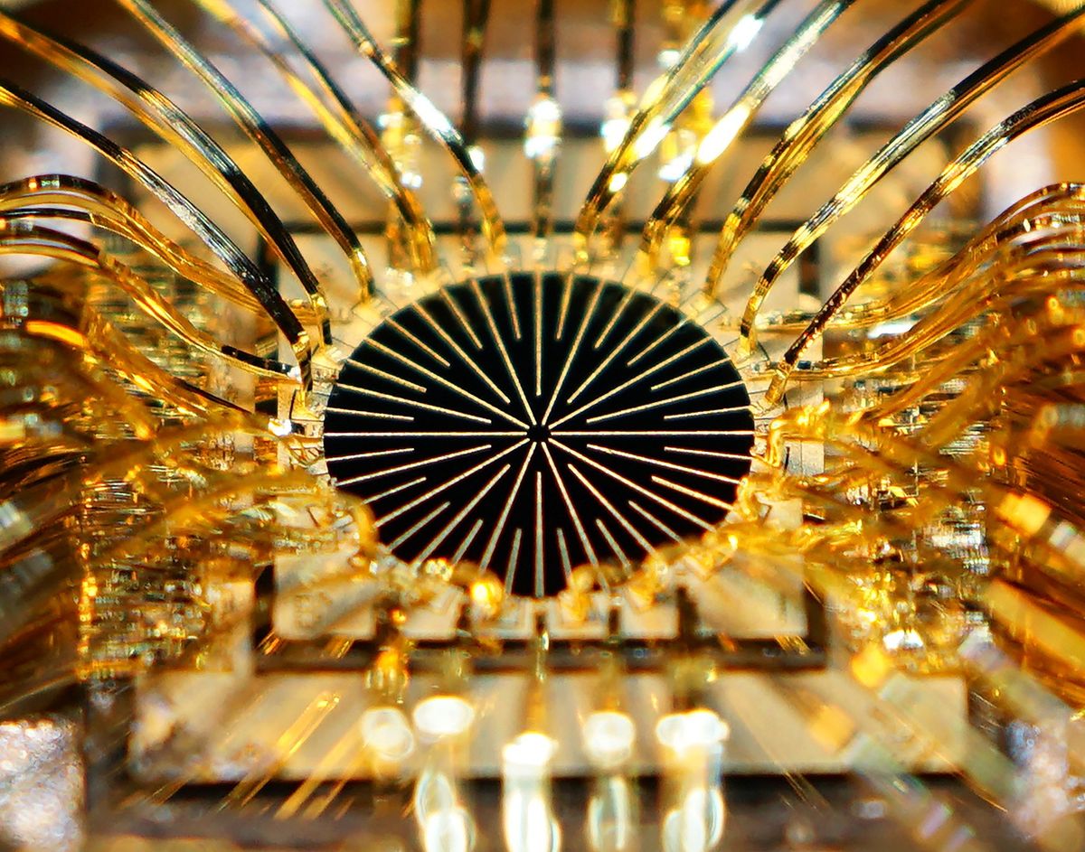
Image: Joshua D. Wood/University of Illinois at Urbana-Champaign