The dominance of resist-based lithography in nanoscale fabrication is being slowly eclipsed by the growing emergence of physical-probe methods, such as electron beam induced deposition or focused ion beam milling.
Now researchers at Oak Ridge National Laboratory (ORNL) have tested the capabilities of one of these physical probe methods, known as helium ion microscopy (HIM), to see whether it may be the way forward in fabricating a next generation of two-dimensional electronic devices.
HIM is similar to other focused-ion-beam techniques in that it uses a scanning beam of helium ions to mill and cut samples. What sets HIM apart is its cleanliness. Milling or imaging with helium or neon is preferred to other ion-beam methods, since these two noble gases aren’t reactive and don’t induce any chemical side effects during the fabrication process. Imaging and milling resolution are also hugely important factors. The helium beam can be strongly collimated offering smaller features—and as a result smaller devices.
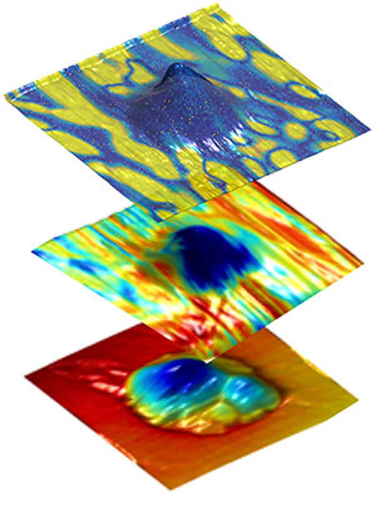
In research described in the journal Applied Materials and Interfaces, the ORNL scientists used the HIM technique to serve as a kind of atomic-scale “sandblaster” on bulk copper indium thiophosphate (CITP). CITP is a ferroelectric material, and the HIM beam was used to introduce localized defects that effect its ferroelectric properties.
While this research only worked with bulk CITP (2-D versions will come later), ferroelecriticy in CITP is very special because this behavior is completely unexpected in a 2-D material. CITP is a layered van der Waals crystal ferroelectric—part of a family of thiophosphate molecules capable of a huge variety of metal substitutions. Besides ferroelectricity, the thiophosphate family offers a number of useful properities including semiconductivity, magnetism, anti-ferroelectricity, and piezoresponse.
By introducing localized defects into the CITP, the researchers discovered it served as a way to manipulate the properties of the material. In particular, the researchers discovered that they could control the distribution of ferroelectric domains in the material as well as enhance its conductivity.
The main point of the research was to look at what properties can be particularly appealing in novel 2-D materials and see how can they be incorporated into the next generation of devices, according to Oak Ridge staff scientist Alex Belianinov.
To this end, the ORNL researchers tested the capabilities of HIM in conjunction with a suite of scanning probe microscopy (SPM) techniques, specifically atomic force microscopy (AFM) band excitation (BE-AFM). What they discovered was that HIM is attractive for nanofabrication because it combines imaging and patterning without poisoning the surface of whatever is being studied with gallium, or other metals typically used in FIB techniques. HIM also offers imaging quality (resolution, field of view, and enhanced channeling effects) that rivals and perhaps exceeds that of scanning electron microscopy (SEM), the workhorse in the field.
“This opens a host of opportunities in clean, direct manufacturing where surfaces can be imaged and modified without a multi-step chemical preparation process,” said Belianinov, in an e-mail interview with IEEE Spectrum. “Additionally, HIM is compatible with direct-write technologies using gas precursors, and in-situ liquid work; both approaches are under intense investigation in the area of electron microscopy to expand material processing arsenal.”
Belianinov added: “HIM is an exceptionally good tool for working with 2-D materials because it can image them, cleanly cut them, (no chemical processing or metal poisoning) and locally induce defects that drastically change material’s properties—as illustrated with the bulk CITP work.”
In future research, the ORNL team will look at tuning the material and synthesizing related compounds with a host of other properties, incorporating the existing materials into functional devices, and continuing to explore the HIM characterization and processing approaches to push novelty and scalability.
Dexter Johnson is a contributing editor at IEEE Spectrum, with a focus on nanotechnology.


