DARPA’s Electronics Resurgence Initiative—a US $1.5 billion five-year effort to remake the U.S. electronics industry as the era of Moore’s Law comes to a close—recently unveiled the scientists, companies, and institutions who are getting its first dose of funds. Among the 42 projects, one stands out for the size of the award.
At $61 million, the Revolutionizing Computing Systems through Dense and Fine-Grained Monolithic 3D Integration project is the largest on the list by nearly $40 million. And its goal is just as outsized: to use monolithic 3D integration to make chips made using decades-old fabrication processes competitive with chips made using today’s bleeding-edge technologies.
The project is based on technology that allows carbon nanotube transistors and resistive RAM memory to be built on top of ordinary CMOS logic chips. It was developed by Max Shulaker, an assistant professor of electrical and computer engineering at MIT, and his colleagues at Stanford University, including Subhasish Mitra and H.-S. Philip Wong.
Last year they unveiled one result, a booze-sniffing multilayer electronic nose made from 2 million carbon nanotube transistors and more than 1 million resistive RAM cells, all built on top of a silicon chip and connected by densely packed metal interconnects between the layers. But what keeps this project from being just another cool demonstration is the involvement of SkyWater Technology Foundry.
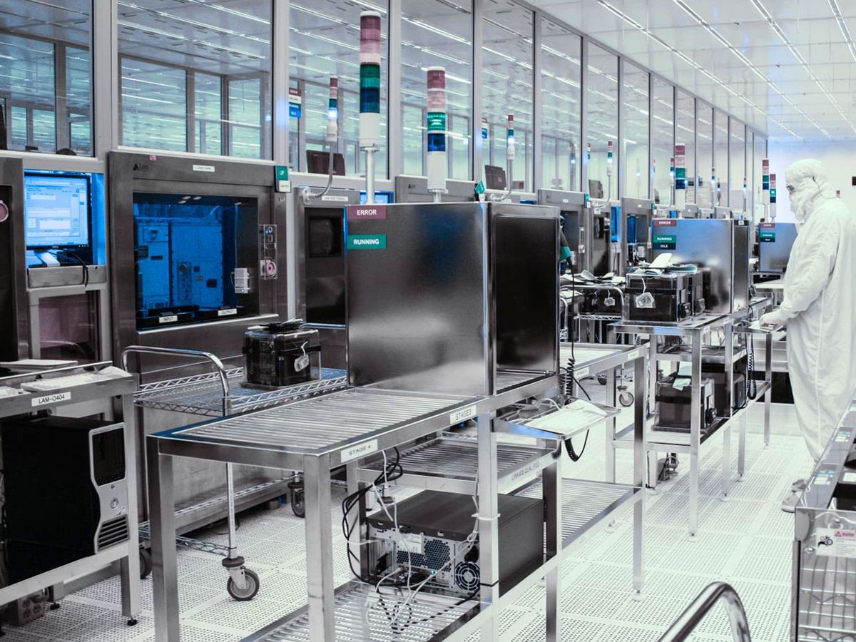
Bloomington, Minn.,-based SkyWater makes chips using 90-nanometer process technology on equipment designed to handle 200-millimeter wafers of silicon. But why would DARPA invest so much in a foundry using a process technology that was cutting edge in 2004 on a size of silicon wafer that big players started to abandon more than 15 years ago?
Listening to the arguments of SkyWater president Thomas Sonderman makes it seem that this foundry is probably not just the best choice but that it might have been the only one.
Because it’s such a reliable process and one that’s widely available for making relatively small volumes of chips, “a lot of the government work is done around 90 nm,” says Sonderman. “So having a technology that can be evolved to higher performance but still follows 90-nm flow is very important.”
DARPA, according to Sonderman, is also keen on keeping the technology in the United States, and SkyWater is now the only American-owned pure-play silicon foundry in the country. If DARPA had chosen to have the process developed in, say, a national lab like Sandia, the result might have relied on uncommon equipment and expertise, and it would still need to be ported to a commercial foundry if it were ever to move beyond defense applications and be used commercially. “Developing the technology in the same fab where you’re going to ramp it [up] gives you a much more manufacturable product,” says Sonderman.

What’s more, it’s not every fab that’s willing to work with nonstandard materials such as carbon nanotubes, which if not properly handled could contaminate the products of other customers.
“There’s a whole protocol you put in place when you want to bring in, say, superconducting materials, and you want to put them on the same line as you’re doing CMOS flows,” explains Sonderman. “Not only have we put those protocols in place but we have around 10 years of experience doing that. I think that’s one of our real advantages and why it’s going to be hard to compete with the SkyWater model.”
Over the next three years, Shulaker’s group at MIT will focus on developing a manufacturable process, and the Stanford group will create design tools that will help engineers take advantage of the increased performance that the stacking of CMOS, nanotube transistors, and RRAM offers. And Skywater will develop and test a high-yield “process flow” that works in its foundry.
“The U.S. government was very interested in standing up a process that not only worked in the lab but could also be offered in a traditional foundry model,” says Sonderman. “Which means you not only have the technology, you create a process to offer to customers.”
Being able to boost performance without going through the very expensive move to a more advanced technology node would be a big win for SkyWater, and eventually other small foundries. The feature-shrinking that’s driven Moore’s Law over the decades is becoming too expensive to continue much longer. The newest processes, depending on extreme-ultraviolet lithography, are billion-dollar investments, says Sonderman. And the volumes needed to keep them afloat aren’t conducive to serving small, Internet-of-Things customers, he argues. “If it all works as planned, it’s like setting the bar back at 90 nm. And we can continue to scale,” he says.
Samuel K. Moore is the senior editor at IEEE Spectrum in charge of semiconductors coverage. An IEEE member, he has a bachelor's degree in biomedical engineering from Brown University and a master's degree in journalism from New York University.


