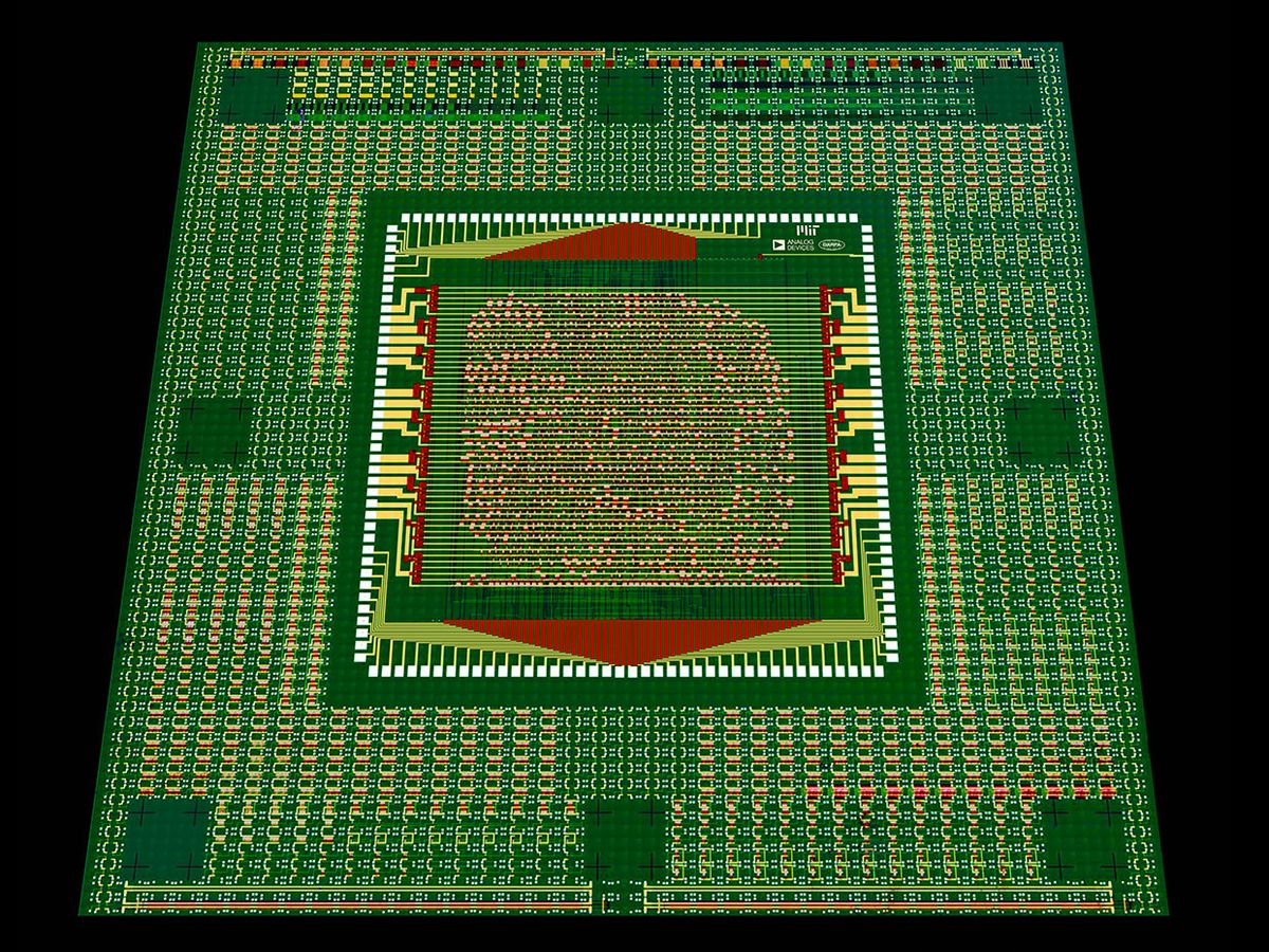
Engineers at MIT and Analog Devices have created the first fully-programmable 16-bit carbon nanotube microprocessor. It’s the most complex integration of carbon nanotube-based CMOS logic so far, with nearly 15,000 transistors, and it was done using technologies that have already been proven to work in a commercial chip-manufacturing facility. The processor, called RV16X-NANO, is a milestone in the development of beyond-silicon technologies, its inventors say.
Unlike silicon transistors, nanotube devices can easily be made in multiple layers with dense 3D interconnections. The Defense Advanced Research Projects Agency is hoping this 3D aspect will lead to commercial carbon nanotube (CNT) chips with the performance of today’s cutting-edge silicon but without the high design and manufacturing cost.
Some of the same researchers created a modest one-bit, 178-transistor processor back in 2013. In contrast, the new one, which is based on the open source RISC-V instruction set, is capable of working with 16-bit data and 32-bit instructions. Naturally, the team, led by MIT assistant professor Max Shulaker, tested the chip by running a version of the obligatory “Hello, World!” program. They reported the achievement this week in Nature.
“Ten years ago, we hoped this was possible,” says Shulaker. “Now we know it is possible… and we know it can be done in commercial facilities.”
Shulaker’s team, along with engineers at Analog Devices and, later, Skywater Technology Foundry, developed three commercially-viable techniques to create the RV16X-NANO. Two dealt with stubborn issues of carbon nanotube purity and uniformity, and the third allowed for the creation of both n-type and p-type transistors to form complementary logic circuits.
1. When making CNT transistors, the nanotubes are first put into a solution and spread across a silicon wafer. Most of the nanotubes lie uniformly on the silicon, but every once in a while, they ball up into bundles of a thousand or more. These bundles can’t form transistors. When building small-scale test circuits, this was no big deal, Shulaker explains, because even if they killed one circuit, another would work. But for a large-scale integration like for the RV16X-NANO these nanotube-pile-ups would be common enough to mess up the whole processor.
RINSE, a solution one of Shulaker’s students, Christian Lau, arrived at, relies on the fact that individual nanotubes are stuck to the substrate by Van Der Waals forces more strongly than bundles are. By first coating the nanotube-covered substrate with a photo resist and then carefully washing it away—under just the right conditions—the process selectively removes the bundles but leaves the individual CNTs.
2. While RINSE dealt with one carbon-nanotube impurity, another purity problem nearly crashed the whole project. CNTs have always come in two basic flavors, metallic and semiconducting. Having some metallic nanotubes in a CNT-based logic gate means the circuit will waste power and produce a noisy signal. But how many metallic nanotubes is too many when you’re trying to build a full-scale processor?
“It’s a very basic question,” says Shulaker. And to his surprise, it hadn’t been answered. The answer his team came up with was “pretty depressing.” The best today’s commercial processes could produce is 99.99 percent semiconducting nanotubes and 0.01 percent metallic. But what’s needed is 99.999999 percent purity—impossibly far out of reach.
“We thought, if we can’t process our way out of this… then somehow we had to design our way around it,” says Shulaker. The team found that, by far, the main driver for the needed purity was not the power issue but the noise. Amongst the many logic circuits they’d made, they found a pattern that suggested some combinations were much more susceptible to the noise problem than others. “So the solution at that point was simple: We’ll just design circuits with the good combinations of logic gates and avoid using the bad combinations.”
DREAM, the set of design rules post-doctoral researcher Gage Hills came up with, allows large-scale integration using carbon nanotubes you can purchase off-the-shelf.
3. The third big breakthrough, called MIXED, allowed for the creation of the two types of transistors needed for CMOS logic, the kind in use in all-kinds of processors for decades. For that you need both electron-conducting (NMOS) and hole conducting (PMOS) transistors. Previous attempts at nanotube processors, such as the one-bit system Shulaker built as a graduate student, used only PMOS.
In silicon, the distinction is achieved by doping the transistor’s channel region with different atoms to effectively add electrons to the silicon crystal lattice or steal some. But such “substitutional doping” doesn’t work for carbon nanotubes. “It’s difficult to swap out an atom without destroying the properties of the nanotube,” says Shulaker.
So instead they turned to “electrostatic doping.” Here, a dielectric oxide is engineered to add or subtract electrons from the nanotube. Using a common semiconductor manufacturing technology called atomic layer deposition, the team was able to deposit dielectrics, such as halfnium dioxide, one atomic layer at a time. By manipulating the exact composition of the layer, say to have slightly fewer oxygens or a bit more, the oxide “wants to either donate electrons to the nanotube or steal from the nanotube,” explains Shulaker.
Between careful selection of the metal electrodes involved and the ALD process, the researchers were able to reliably build PMOS and NMOS devices together.
Crucially, MIXED is a low-temperature process, so the transistors can be built on top of other layers of circuitry without damaging them. In fact, the transistors in RV16X-NANO were built in between a layer of interconnects that provide power to the transistors and another layer that connects the transistors into logic gates and larger systems. Engineers are interested in such “buried power line” schemes in order to free up space that would allow for better-performing or smaller systems. But they are more difficult to achieve in silicon, in part because of high processing temperatures.
A version of this post appears in the October 2019 print issue as “Finally, a Functional Carbon-Nanotube CPU.”
