Lithium niobate (LiNbO3) is a hard, chemically inert, crystalline material with exceptional optical properties. Because of these properties, it has found a niche of sorts in electro-optics, acousto-optics, and nonlinear optics.
Components made of this material are now found in a wide range of devices, including cellphones, optical modulators, and frequency converters. However, unlike silicon, which is easy to etch, lithium niobate is not amenable to chemical etching, a technique used in the silicon-based industry to produce nanometer-size structures like waveguides.
Other techniques used to create waveguides, such as ion diffusion and proton exchange, were unsuitable for lithium niobate because they resulted in a low optical-index contrast between the waveguide and the bulk material. A high optical-index contrast is important to allow the propagation of light through the waveguides etched in lithium niobate because this would allow manufacturers to fully exploit the optical properties of the material.
One way to resolve this difficulty could be a hybrid approach, explored at several research centers during the last few years: combine the ease of etching in silicon with the optical properties of lithium niobate thin films. In a sandwich of lithium niobate and silicon, the waveguides etched in the silicon surface would guide the light through the lithium niobate, where it could exploit the material’s transparency and nonlinear optical properties.
Unfortunately, the coupling between the light passing through the silicon waveguides and the lithium niobate proved to be too low to be practical.
Researchers at Harvard University recently published a study in Optica about how their experience with similar intractable materials inspired them to apply another technique—plasma reactive ion etching.
Plasma reactive ion etching is the bombardment of the surface of a chip with ions, whereby sections exposed by a patterned mask are removed by the chemical interaction of the ions with atoms on the surface of the chip.
“Over the years, we have dealt with many materials that have nice properties but that are difficult to work with,” says Marko Lončar, who led the research. One of these materials is diamond. “Diamond is actually easier to etch than niobate, but it doesn’t exist as thin films,” says Lončar.
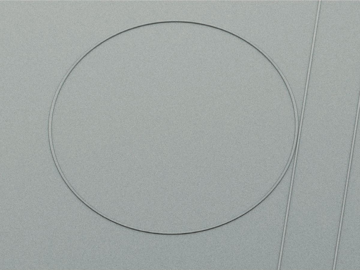
As a demonstration of this new approach to etching nanostructures, the researchers created a micro-ring and a few micro-racetracks about 1 micrometer wide, with a curvature radius of 80 µm.
The first step was not different from standard silicon etching. They etched the patterns for the waveguides with electron-beam lithography on a photoresist layer. Then they transferred the obtained mask onto the niobate film, whereby it protects sections of the underlying film from being etched away. Finally, they used plasma reactive ion etching to direct a beam of argon ions on the sample, removing material from the strips exposed by the resist layer and forming trenches that become the waveguides.
With their new waveguide, the researchers found that optical power losses over a distance of 1 meter would only be 50 percent, as compared with the 99-percent loss observed in previous lithium niobate devices. They explain in a press release that an important improvement in optical confinement, to prevent the leaking of light through the edges of the waveguide, contributes to this. “If you have high confinement, you can bend the light over a smaller radius,” says Lončar.
Marco Bazzan, a material scientist at the University of Padova, in Italy, agrees that the result is remarkable. “If confirmed, this result would place lithium niobate resonators on a higher ground, even with respect to standard silicon photonic devices,” he says. “Such a good performance, coupled with the nonlinear optical properties of lithium niobate, gives a lot of importance to this work, especially in the forthcoming era of integrated quantum photonics,” he adds.
Moving toward integrated silicon photonics is exactly how Lončar’s team sees the future of this research. But to achieve this, they plan to return to the hybrid model.
“The next step is the integration of the niobate into silicon photonic processing, and that may be challenging because niobium is not a material people in the silicon industry like very much. Maybe we will have to turn to dedicated fabrication facilities that will allow this hybrid electronic integration,” says Lončar. “For now, we have to make the niobium chips and the silicon chips separately and couple them together,” he adds.
However, Bazzan is optimistic. “The thin film substrates used for this investigation are not produced in a research laboratory but bought from a commercial company. This means that the technological steps are already ready for standardization,” he says.
Editor’s note: This story was updated on 16 January 2018.


