While inventors of digital electronic applications are still wrestling with graphene’s lack of a band gap, in optoelectronics the wonder material is more popular than ever. This is no more apparent than in photodetectors, where graphene’s properties as an extreme-broadband absorber enables photodetection for visible, infrared, microwave and terahertz frequencies all while providing very high photo-response speeds.
Despite all this great promise, research has been somewhat limited by the fact the photoresponse only occurs at specific locations on the graphene that represent a relatively small area compared to the entire photodetector.
Now researchers at Purdue University have found a way to work around this limitation, and the result could mean getting sharper images even with fewer photodetector pixels.
In work described in the journal Nature Nanotechnology, the Purdue researchers designed their photodetector so that the light interaction and absorption occurs on the substrate of the device—underneath the graphene. In this design, the substrate is much larger than the graphene so the photoresponse area is much larger, and also provides greater positional sensitivity to where the photons are landing on the device.
“Our device with large photoresponse area and position sensitive response may be particularly valuable for those applications where the light may come from an unknown or random direction before detection,” explains Yong Chen, a professor of physics and astronomy at Purdue and co-author of the research, in an e-mail interview with IEEE Spectrum.
Examples of where these properties might be of particular importance would include astronomy—or in a quite disparate area, the detection of radiation from concealed sources in security applications.
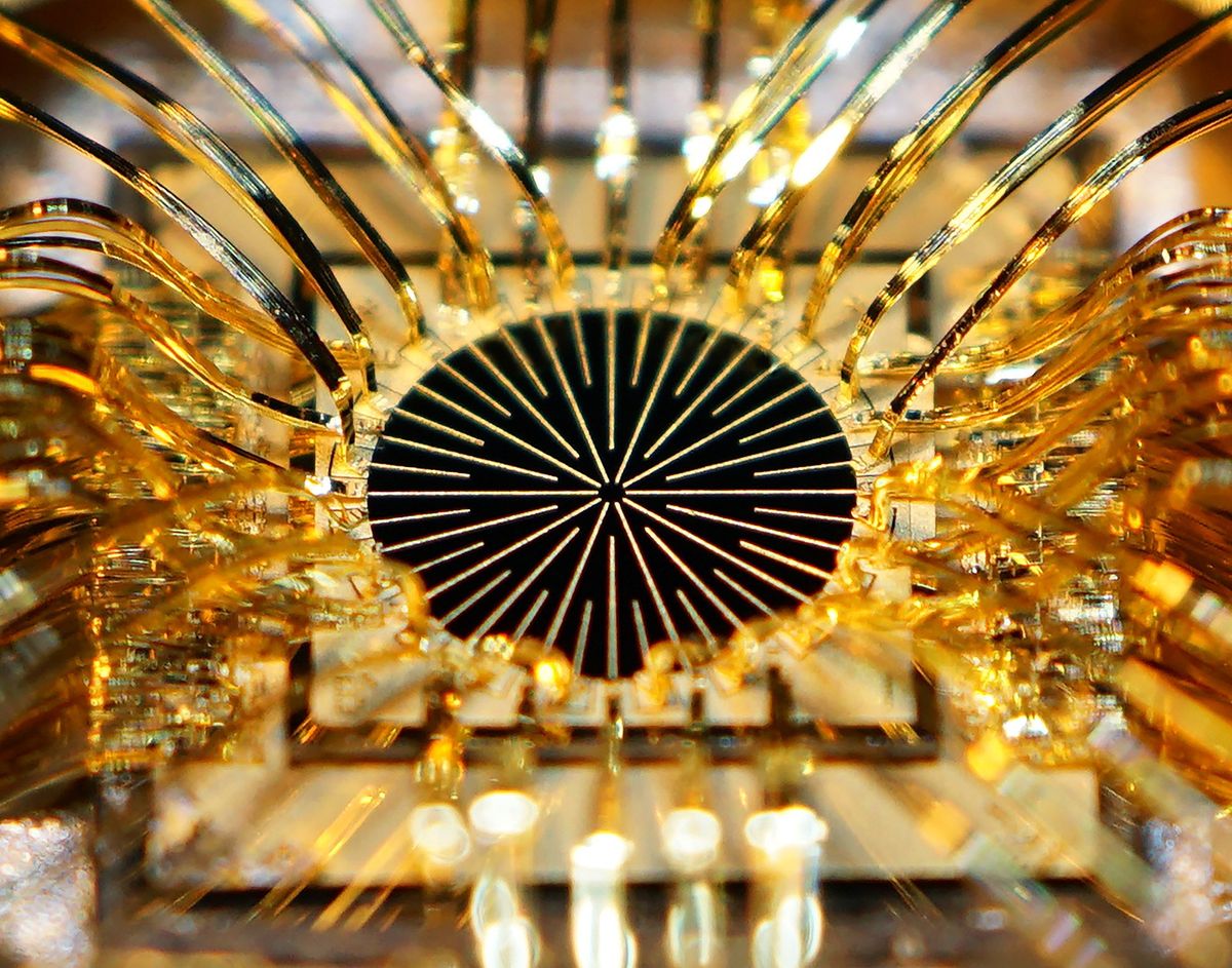
The main element of the photodetector is a back-gated graphene field-effect transistor (GFET). While back-gated devices—in which the gate electrode lies beneath a layer of insulation and the graphene lies atop the insulation—are generally more difficult to integrate to form complex circuits, many of the earlier designs for photodetectors also employed back gates, according to Chen.
Chen explains that previous back-gated devices typically used a doped silicon substrate, which is not involved in the light interaction. This latest device uses an undoped silicon carbide substrate with a metal back gate. With a voltage at the back gate, light striking the substrate modulates the conductivity of the graphene. All other things being equal, how much the the light modulates the conductivity depends on how far from the graphene it strikes. So you can read out the position by running current through the graphene.
“The much larger size of this photo-sensitive substrate and back gate gives the large response area,” says Chen. “We further found that the response depends on the location of where the photons land on the SiC substrate away from the graphene. This gives rise to the position sensitivity.”
While previous graphene photodetectors could achieve large area and position-sensitive detection if they were built into a dense array of many graphene pixels, it would come at the cost of fabrication complexity. “Our non-local ‘field effect’ based photodetection offers a different, and much simpler approach where even a single graphene device can achieve large response area and position sensitivity,” says Chen.
Chen concedes that you may still need an array of such detectors to further improve the spatial resolution and position sensitivity in future applications, but with the new graphene detectors the density and number of pixels needed is likely to be comparatively small.
Chen is quick to point out that this latest research should really only be considered an early-stage demonstration. “Many aspects can be further improved for real world deployment,” he says. “For example, the response speed is still relatively slow in these devices (with rise/fall time ranging from milliseconds to many seconds) and the initial applications may be more geared to those where a high speed operation is not critical.”
In addition to improving the response time, Chen and his colleagues are looking to further improve the quality of materials, including the photosensitive substrate, the graphene itself, as well as the graphene-substrate interface. Chen believes that improving the materials could go a long way to boosting the response speed as well as the repeatability and reliability of the device response.
Dexter Johnson is a contributing editor at IEEE Spectrum, with a focus on nanotechnology.