It was a eureka moment when IBM researchers first realized that they were imaging the surface of an atom with what came to be known as the scanning tunneling microscope (STM). Many believe that invention triggered the field of nanotechnology. Now researchers at the University of California Santa Barbara (UCSB) have created a next-gen microscope that can image phenomena like magnetism on the atomic scale across a huge range of temperatures. The heart of the microscope is a single atom or, perhaps more accurately, the absence of a single atom.
In research described in the journal Nature Nanotechnology, the researchers fabricated a new kind of microscope sensor based on something called a nitrogen–vacancy (NV) defect in diamond. In these NV defects, a nitrogen atom replaces a carbon atom at one point in the diamond’s molecular lattice. This disrupts the structure of the lattice and leaves empty a normally-occupied location adjacent to the nitrogen atom.
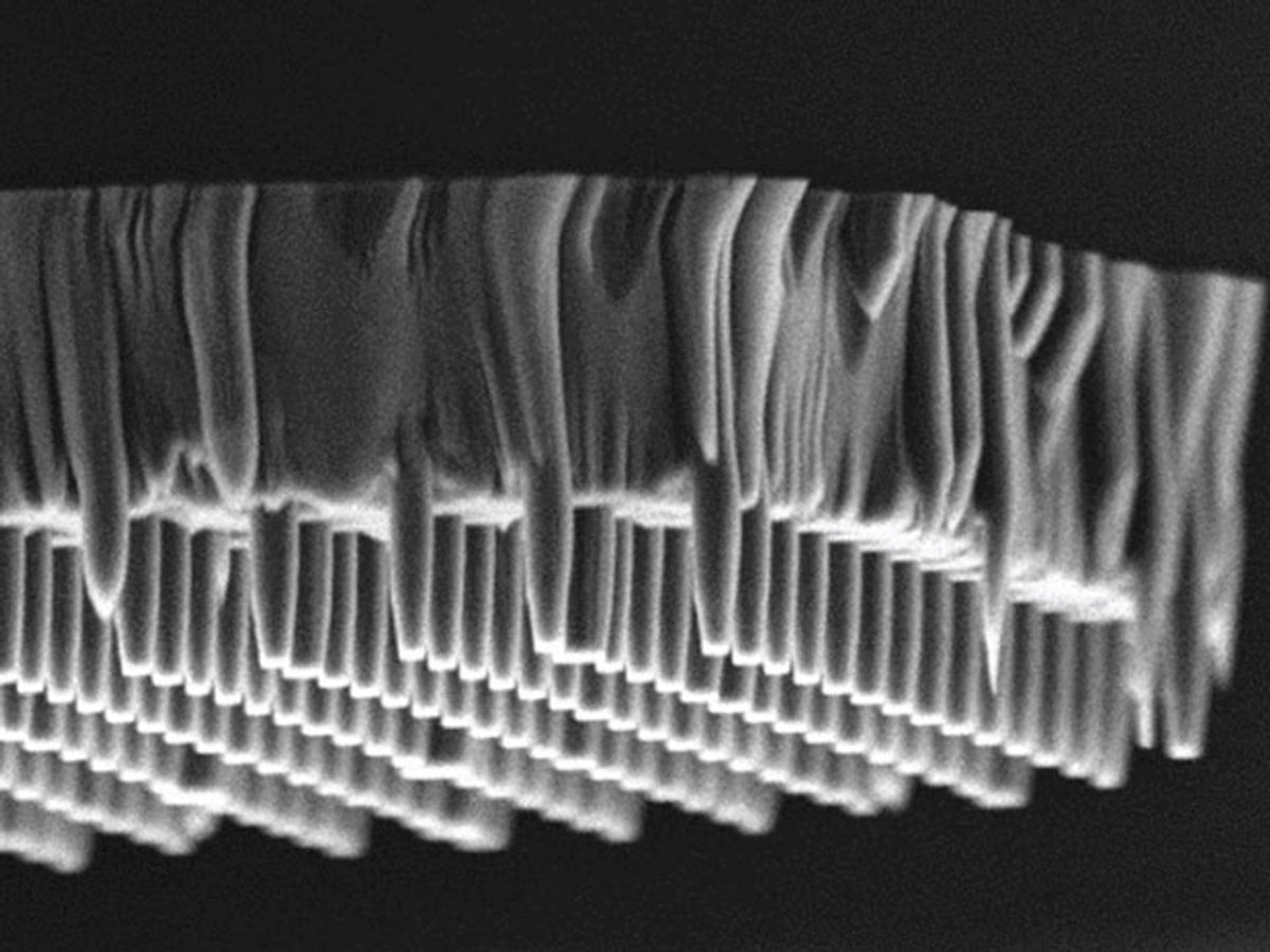
This defect in the diamond lattice makes possible the sensing of certain physical phenomenon, most notably magnetism. In operation, a NV-based magnetic sensor detects this magnetism by measuring the defect’s spin-dependent photoluminescence. To actually build a microscope, the UCSB researchers created a sensor that resembles a toothbrush. Each bristle in this toothbrush-like structure has one of these NV defects at the tip.
“This is the first tool of its kind,” said Ania Jayich, a professor and leader of the research, in a press release. “It operates from room temperature down to low temperatures where a lot of interesting physics happens. When thermal energy is low enough, the effects of electron interactions, for instance, become observable, leading to new phases of matter. And we can now probe these with unprecedented spatial resolution.”
To test their NV-based sensor, the researchers imaged a superconductor that contained magnetic structures known as vortices, which are areas of changing magnetic flux. The new sensor was able to discern individual vortices.
In continuing research, the UCSB team is exploiting this excellent resolution to look at the world of skyrmions, which are swirling magnetic spin patterns in thin films. Skyrmions may sound obscure but they more form the basis a new kind of data storage. With this new NV-based sensor, the researchers believe that its high resolution will make it possible to image all the interactions that occur in a material that lead to skyrmions.
Jayich added: “There are a lot of different interactions between atoms and you need to understand all of them before you can predict how the material will behave.”
Dexter Johnson is a contributing editor at IEEE Spectrum, with a focus on nanotechnology.


