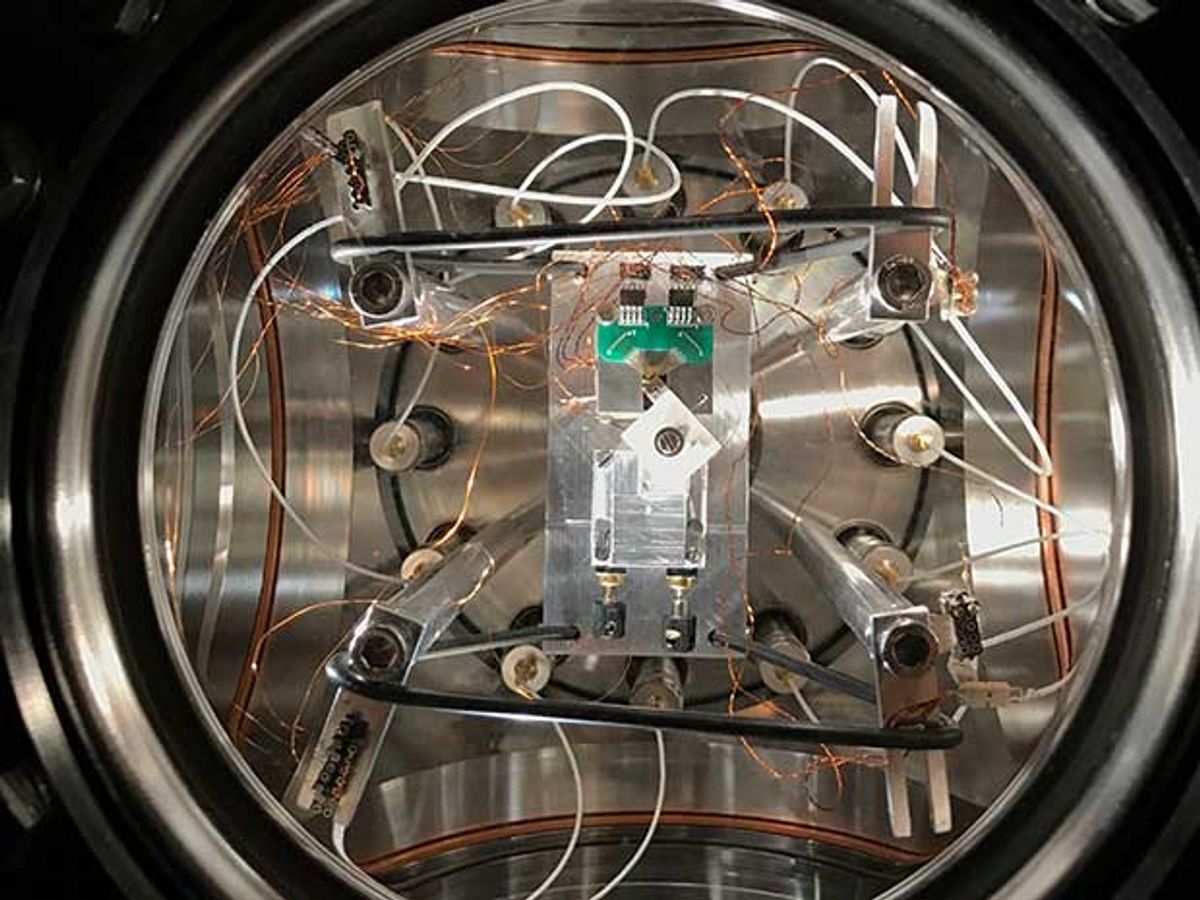
IBM researchers have established experimental proof of a previously difficult-to-prove law of physics, and in so doing may have pointed to a way to overcome many of the heat management issues faced in today’s electronics. Researchers at IBM Zurich have been able to take measurements of the thermal conductance of metallic quantum point contacts made of gold. No big deal, you say? They conducted measurements at the single-atom level, at room temperature—the first time that’s ever been done.
The first measurement of a quantum of thermal conductance was achieved back in 1999 by researchers at the California Institute of Technology. This latest research differs in that it was able to make measurements at room temperature as opposed to very low temperatures.
These latest measurements provide further confirmation of the Wiedemann–Franz law, which predicts that the smallest amount of heat that can be carried across a metallic junction—a single quantum of heat—is directly proportional to the quantum of electrical conductance through the same junction. By experimentally confirming this law, it can now be used with confidence to predict and to explore nanoscale thermal and electrical phenomena affecting materials down to the size of few atoms or a single molecule.
“Although the Wiedemann–Franz law is predicted, and should be valid for certain metals, it has turned out to be difficult to prove it when you go to the nanoscale,” explained Bernd Gotsmann, an IBM scientist and one of the lead researchers on this work, in an e-mail interview with IEEE Spectrum. “We think the difficulty is mainly a sign of the challenges related to the measurement of thermal transport on small scales.”
In research described in the journal Nature Nanotechnology, the IBM Zurich team was able to achieve this experimental confirmation by employing a relatively new microscopy technique that had been developed at its lab just last year: scanning probe thermometry.
This technique essentially combines thermal sensing with the measuring capability of a microscope. The resulting device flipped all previous attempts to take these measurements on their head; instead of attempting to fabricate a nanoscale thermometer, they produced a thermometer for the nanoscale.
In operation, the tip of an atomic-force microscope (AFM) is used to measure two signals simultaneously: a small heat flux, which is the thermal energy being transferred through the surface of the material; and the resistance of the material to heat flow. By combining these two measurements, it becomes possible to determine how much heat is locally present on a nanoscale device. You can see a video describing the measurement device below.
However, amazing as that new scanning probe thermometer was, it was initially still unable to resolve the single quantum of heat for objects smaller than around 10 nanometers. Now the same team of researchers has improved its sensitivity down to the scale of one atom, which is around 0.1 to 0.3 nanometers depending on the element.
Key to the achievement was the development of a microelectromechanical system (MEMS) that included an integrated thermal sensor that is operated within a vacuum-based scanning tunneling microscope (STM). Another important factor was the availability of IBM’s Noise Free Lab in Zurich (which I toured while it was under construction back in 2010 and a year later when it went into operation). The lab is protected from nearly any type of disturbance—including the earth’s magnetic field or vibrations from a train passing nearby.
The development of the thermal sensor was probably the most challenging part of the work, according Gotsmann.
“Measuring how heat is created and transported at the nanoscale is very challenging,” says Gotsmann. “In particular, the fabrication of our thermal sensors has been a major hurdle. They must be sensitive enough to feel the touch of a single atom and at the same time stiff enough to keep such contact stable during the (painfully slow) measurement time.”
The new system operates much like the previous iteration of the scanning probe thermometer, in that it combines simultaneous measurements of heat and charge transport to determine the thermal and electrical conductance of metallic contacts. In this case, the STM tip is used to form and break contacts on a substrate covered by a metallic layer. This is similar to other STM break-junction set-ups, but here, the bottom electrode is integrated on a suspended MEMS to insulate it thermally from the chip substrate.
The IBM researchers first use of this technique will be to study how atomic bonds can contribute to the thermal coupling between materials. This is critical for thermal management because, at the nanoscale, thermal resistance is dominated by the interfaces between materials. “It seems that the properties of the interface on the scale of the first atomic layers at the interface can be extremely important,” adds Gotsmann.
The IBM team believes there are many directions to go with this measurement technique. In the Nature paper, the researchers contend: “This will enable heat transport to be investigated not only in quantum point contacts of different metals, but also in molecular junctions, a fundamental scientific and technological step forward in managing and controlling heat at the nanoscale.”
This post was corrected on 9 February to include mention of Cal Tech’s original measurement of a quantum of thermal conductance.
Dexter Johnson is a contributing editor at IEEE Spectrum, with a focus on nanotechnology.


