IBM’s $3-Billion Research Project Has Kept Computing Moving Forward
With IBM’s “7-nm and Beyond” research initiative completed, it's time to assess how its innovations have helped chipmakers keep up with the demands of Moore’s Law
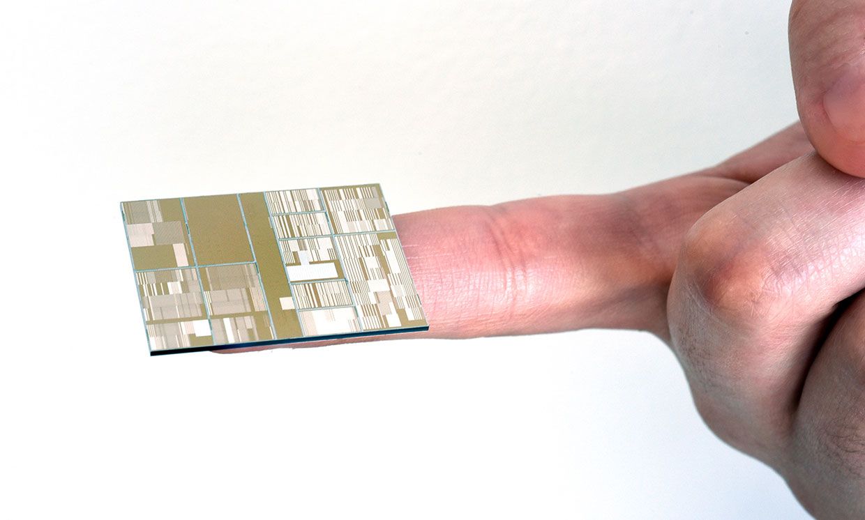
Back in 2014, under the looming shadow of the end of Moore’s Law, IBM embarked on an ambitious, US $3 billion project dubbed “7-nm and Beyond”. The bold aim of that five-year research project was to see how computing would continue into the future as the physics of decreasing chip dimensions conspired against it.
Six years later, Moore’s Law isn’t much of a law anymore. The observation by Gordon Moore (and later the industry-wide adherence to that observation) that the number of transistors on a chip doubled roughly every two years seems now almost to be a quaint vestige of days gone by. But innovation in computing is still required, and the “7-nm and Beyond” project has helped meet that continuing need.
“The search for new device architectures to enable the scaling of devices, and the search for new materials for performance differentiation will never end,” says Huiming Bu, Director at IBM’s Advanced Logic & Memory Technology Research, Semiconductor, and AI Hardware Group.
Although the chip industry may not feel as constrained by Moore’s Law as it has in the past, the “7-nm and Beyond” project has delivered important innovations even while some chip manufacturers have seemingly thrown up their hands in frustration at various points in recent years.
One example of this frustration was the decision two years ago by GlobalFoundries to suspend its 7-nanometer chip development.
Back in 2015, one year into its “7-nm and Beyond” project, IBM announced its first 7-nm test chip in which extreme-ultraviolet lithography (EUV), supplied by ASML, was a key enabling technology. While there have been growing pains in the use of EUV—resulting in the richest chip manufacturers being the only ones continuing on with the scaling down that it enables—it has since become a key enabling technology not only for 7-nm nodes, but also for 5-nm nodes and beyond, according to Bu.
“Back in the 2014-2015 time window, the whole industry had a big question about the practical feasibility of EUV technology,” says Bu. “Now it's not a question. Now, EUV has become the mainstream enabler. The first-kind 7-nm work we delivered based on EUV back then helped to build the confidence and momentum towards EUV manufacturing in our industry.”
Of course, EUV has enabled 7-nm nodes, but the aim of IBM was to look beyond that. IBM believes that the foundational element of chips to enable the scaling beyond FinFET will be the nanosheet transistor, which some have suggested may even be the last step in Moore’s Law.
The nanosheet looks to be the replacement to the FinFET architecture, and is expected to make possible the transition from the 7-nm and 5-nm nodes to the 3-nm node. In the architecture of the nanosheet field-effect transistors, current flows through multiple stacks of silicon that are completely surrounded by the transistor gate. This design greatly reduces the amount of current that can leak during off state, allowing more current to be used in driving the device when the switch is turned on.
“In 2017, the industry had a question about what will be the new device structure beyond FinFET,” says Bu. “At this point, three years later, the whole industry is getting behind nanosheet technology as the next device structure after FinFET.”
The transistors and switches have had some key developments, but the “7-nm and Beyond” project also resulted in some significant insights into how the wiring above all these transistors and switches will be made going into the future.
“Part of our innovation has been to extend copper as far as possible,” says Daniel Edelstein, IBM Fellow; Si Technology Research; MRAM/BEOL Process Strategy. “The hard part, as always,” says Edelstein, “has been simply patterning these extremely tiny and tall trenches and filling them without defects with copper.”
Despite the challenges with using copper, Edelstein doesn’t see the industry migrating away from it to more exotic materials in the near future. “Copper is certainly not at the end of its rope for what's being manufactured today,” said Edelstein.
He adds: “Several companies have indicated that they intend to continue using it. So I can't tell you exactly when it breaks. But we have seen that the so-called resistance crossover point keeps getting pushed farther into the future.”
While chip dimensions, architectures and materials have driven much of the innovations of the “7-nm and Beyond” project, both Edelstein and Bu note that artificial intelligence (AI) is also playing a key role in how they are approaching the future of computing.
“With the onset of AI-type, brain-inspired computing and other kinds of non-digital computing, we're starting to develop, at the research level, additional devices—especially emerging memory devices,” says Edelstein.
Edelstein is referring to emerging memory devices, such as phase-change memory (or “memristors,” as some others refer to them), which are thought of as analog computing devices.
The emergence of these new memory devices has provided a kind of resurrection in thinking about potential applications over and above conventional data storage. Researchers are imagining new roles for the thirty-year-old magnetoresistive random-access memory (MRAM), which IBM has been working on since MRAM’s debut.
“MRAM has finally had enough breakthroughs where it’s now not only manufacturable, but also approaching the kinds of requirements that it needs to achieve to be competitive with SRAM for system cache, which is kind of the holy grail in the end,” says Edelstein.
The evidence of this embedding of MRAM and other nonvolatile memories—including RRAM and phase-change memory—directly into the processor is seen in the move last year by chip equipment manufacturer Applied Materials to give its customers the tools for enabling this change.
The pursuit of new devices, new materials, and new computing architectures for better power-performance will continue, according to Bu. He also believes that the demand to integrate various components into a holistic computing system is starting to drive a whole new world of heterogeneous integration.
Bu adds: “Building these heterogeneous architecture systems is going to become a key in future computing. It is a new innovation strategy driven by the demands of AI.”
Dexter Johnson is a contributing editor at IEEE Spectrum, with a focus on nanotechnology.