Four years ago, IBM announced that it was investing US $3 billion over the next five years into the future of nanoelectronics with a broad project it dubbed “7nm and Beyond.” With at least one major chipmaker, GlobalFoundries, hitting the wall at the 7-nm node, IBM is forging ahead, using graphene to deposit nanomaterials in predefined locations without chemical contamination.
In research described in the journal Nature Communications, the IBM researchers for the first time electrified graphene so that it helps to deposit nanomaterials with 97% accuracy.
“As this method works for a wide variety of nanomaterials, we envision integrated devices with functionalities that represent the unique physical properties of the nanomaterial,” said Mathias Steiner, manager at IBM Research-Brazil. “We also can envision on-chip light detectors and emitters operating within a distinct wavelength range determined by the optical properties of the nanomaterial.”
As an example, Steiner explained that if you wanted to modify the spectral performance of an optoelectronic device, you could simply replace the nanomaterial while keeping the manufacturing process flow the same. If you take the method one step further, you could assemble different nanomaterials in different places doing multiple passes of assembly to create on-chip light detectors operating in different detection windows at the same time.
The entire method can be considered a hybrid bottom-up/top-down process flow, according to Michael Engel, research staff member at IBM Research–Brazil. A couple of years ago, IBM created one of these hybrid processes that combined top-down manufacturing techniques—like lithography—with bottom-up techniques that “grow” electronics through self-assembly.
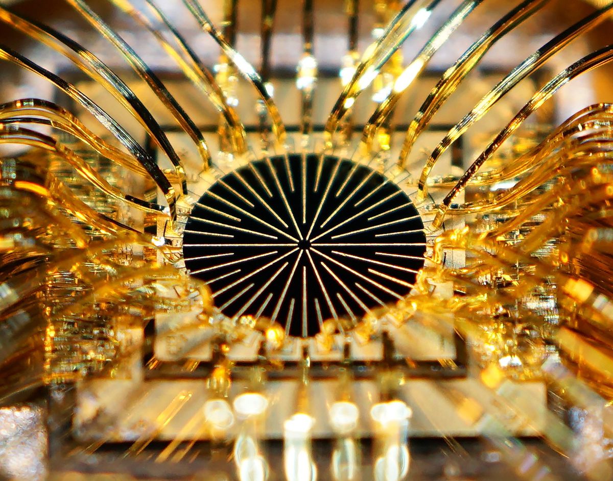
Engel explained that the first step of this hybrid process involves growing graphene directly on top of the substrate where the nanomaterial assembly is performed.
In IBM’s demonstration, they used graphene on silicon carbide. Engel noted that it is also possible to grow the graphene on another material, such as copper, then peel the graphene off and put it on a silicon/silicon oxide wafer.
The next step was etching the graphene to define the deposition sites. This is done at a large scale and can be considered the top-down part of the process.
The third step employs a bottom-up technique where researchers apply an AC electric field to the patterned graphene layers while depositing nanomaterial solution on top. The nanomaterial is then dragged down and trapped between opposing graphene electrodes.
“So the graphene fulfills the function of defining the placement location and providing the electric field orientation and drag force for the directed nanomaterial assembly,” said Engel.
In the fourth step of this process, the graphene deposition electrodes are etched away, followed by additional manufacturing steps for integrating and operating electronic or optoelectronic devices.
The state of the art prior to this work was using metal electrodes, which are difficult to remove and limit device performance and integration potential.
“We believe the biggest breakthrough of this work is the bottom-up placement of a wide variety of nanomaterials with nanometer-scale resolution over much larger, millimeter-scale areas with easily removable (residual free) electrodes,” said Steiner. “The graphene electrodes provide excellent nanomaterial alignment and density, limit chemical exposure, and avoid metal lines, enabling superior device performance.”
This process is not going to come to the rescue of Moore’s Law overnight. One of the biggest challenges, according to Engel, is introducing solution-based nanomaterials into the industrial-scale manufacturing process.
“This will require progress in the standardization of nanomaterial solutions to achieve repeatable and consistent results, as well as the adaption of the electric-field-assisted method for use in the wafer scale manufacturing processes,” said Engel.
While standardization of nanomaterial solutions is not going to be solved by IBM, the researchers are continuing to work on the device level of the technology with the integration of different nanomaterials in order to customize basic integrated circuits such as, for example, electrical inverters or ring oscillators.
Along these lines, the researchers are developing dedicated on-chip light emitters and detectors with spectral properties determined by the assembled nanomaterial.
Editor’s Note: A small change was made on October 9th to correct the mistaken description that the graphene was peeled off of silicon carbide and put onto a silicon/silicon oxide wafer. These are actually two different embodiments of the method: either graphene is grown on silicon carbide (where it stays in place for further processing), or the graphene is grown on copper and transferred to the wafer for further processing.
Dexter Johnson is a contributing editor at IEEE Spectrum, with a focus on nanotechnology.