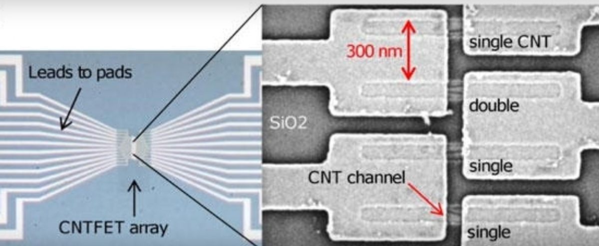
Researchers at IBM’s T. J. Watson Research Center in Yorktown Heights, New York are reporting success in precisely locating a high density of carbon nanotubes on a substrate that should lead to high-speed and power-efficient chips and could show a way forward after silicon.
The IBM team was able to successfully place over 10,000 working transistors on the surface of a silicon wafer. Some anticipate that this research will not only allow the building of smaller transistors but also improve the clock speed of the transistors.
The research, which was published in Nature Nanotechnology (“High-density integration of carbon nanotubes via chemical self-assembly”), was hinted at last year during the IEEE International Electron Devices Meeting (IEDM).
At the IEDM meeting last year there was a lot of noise about IBM demonstrating the first transistor with sub-10nm channel lengths. The tie into that line of research and this latest work is that the IBM team built those sub-10nm nanostructures out of carbon nanotubes and grew them through self- assembly on standard 200-millimeter diameter wafers.
The latest research used ion-exchange chemistry to trigger a chemical self-assembly process for the nanostructures. The researchers place the carbon nanotubes in a solution that makes them water-soluble. Then the carbon nanotubes chemically self assemble onto the substrate in patterned arrays.
The process made it possible to place the carbon-nanotube transistors in a density high enough that the resulting material outperformed any other switches from any other material, according to Supratik Guha, director of physical sciences at IBM’s Yorktown Heights research center in a New York Times article covering the research. “We had suspected this all along, and our device physicists had simulated this, and they showed that we would see a factor of five or more performance improvement over conventional silicon devices,” says Guha in the article.
What might be the most impressive aspect about the results is that the researchers were able to electrically test the 10,000 transistors. Being able to characterize this large a number of nanotube devices is critical for analyzing transistor performance and yield.
This step will also prove crucial in what remains to be the biggest obstacle for the technology in replacing silicon: achieving carbon nanotube purity. At the moment, the carbon nanotubes the researchers have access to contain enough metal in them that they don’t make ideal semiconductors. The IBM team are confident that they can reach a 99.99 percent pure form of carbon nanotubes that will make the devices operate even better than their current prototypes.
Image courtesy of Nature Publishing
Dexter Johnson is a contributing editor at IEEE Spectrum, with a focus on nanotechnology.


