Graphene might be the best conductor of electrons we know. However, as a pure conductor it can’t stop the flow of electrons the way a semiconductor like silicon can. Silicon’s ability to create an on/off state for the flow of electrons makes it possible to create the “0” and “1” of binary digital logic for computing.
While many believe this has pretty much taken graphene out of the running for digital logic applications that depend on turning the flow of electrons on and off, it hasn’t stopped researchers from looking to see if there’s a way to engineer a bandgap into it that will make graphene behave like a semiconductor. The pressure of Moore’s Law on silicon is too great not to look for a solution from every corner.
The problem with these engineered bandgaps is that they come at the cost of compromising the electronic properties of graphene that were so attractive in the first place—most notably its high conductivity.
Now a team of researchers at Columbia University has developed a graphene-based material that has a significant bandgap without coming at the cost of sacrificing its attractive electronic properties.
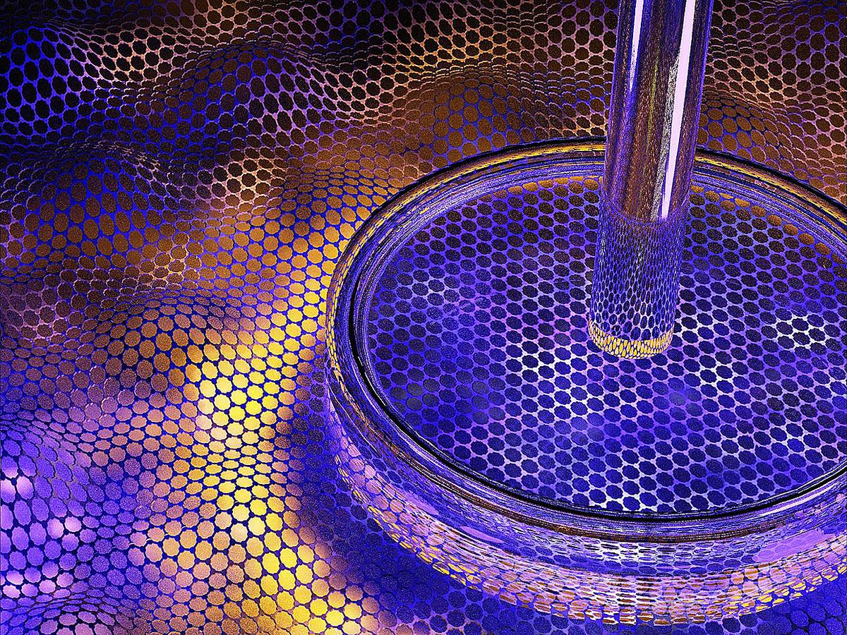
In research described in the journal Nature, the Columbia researchers have created what’s known as a van der Waal (vdW) heterostructure—a combination of different two-dimensional (2D) materials held together by atomic scale forces known van der Waal forces. The researchers have provided a new level of understanding about why bandgaps emerge in these vdW heterostructures, and how to modify the stacking between the 2D layers to open a much larger bandgap, potentially even without pressure.
The researchers experimented with vdW heterostructures consisting of graphene encapsulated between two flakes of boron nitride, an insulator. The new technique employed is to apply hydrostatic (uniform) pressure to this stack of layered 2D materials. They do this with an apparatus called a “piston-cylinder pressure cell.”
“Effectively, the heterostructure sits in a bath of oil inside a Teflon cup, and this cup is compressed so that everything inside feels a uniform high pressure,” explained Matthew Yankowitz, a postdoctoral research scientist at Columbia and lead author of the research.
This application of pressure squeezes all the 2D layers of the heterostructure closer to one another, according to Yankowtiz.
“This is the most important point of the study—we’ve known for years that stacking various 2D materials on top of one another can result in emergent electronic properties distinct from those found in any of the constituent materials alone, and this effect arises from the electronic coupling between the different layers of neighboring materials,” said Yankowitz. “Applying pressure now allows us to tune the strength of this interlayer electronic coupling—and as a result, tune the properties of the vdW heterostructure—by controlling how closely the 2D layers sit with respect to one another.”
In general, for bandgaps to be effective in stopping the flow of electrons for use in transistors, the electron volts (eV)—a measurement of the magnitude of the energy barrier for which electrons cannot conduct electricity through the material—should be much larger than the energy of thermal fluctuations of electrons at room temperature. For instance, in silicon the bandgap is about 1.1 eV, while room temperature fluctuations are about 0.025 eV.
Yankowitz concedes that with their new approach they have only been able to achieve bandgaps of just over 0.05 eV, which is still far from large enough to be useful. However, it is a significant increase over previous graphene/boron nitride vdW heterostructures that have only reached 0.035 eV. While still far from the 1.1 eV bandgap of silicon, Yankowitz sees this research as a good first step.
“Our results suggest that by applying even more pressure we could make the gap much larger still,” said Yankowitz. “More importantly, we have a much clearer understanding of why this gap exists in the first place, which could help us more efficiently target ways to enhance it even without using pressure.”
Recent research out of Spain has demonstrated that it’s possible to grow graphene from the “bottom up” so that it starts off having a bandgap similar to silicon’s 1.1 eV.
Yankowitz is impressed with this line of research, especially since they reported that they have demonstrated a proof-of-principle device based on the material that works at room temperature. However, Yankowitz points out that they have had to induce significant disorder into the graphene lattice, sacrificing its intrinsically high electronic quality.
“Ideally, we would want a large gap while retaining the pristine, disorder-free graphene lattice,” said Yankowitz. “Our work drives towards this, but unfortunately the gap remains too small to even think about creating a device that works at room temperature right now, and it's not immediately obvious how we could do this.”
In future research, Yankowitz and his colleagues will be testing other 2D materials exhibiting a wide range of desirable electronic properties. It is the mix and match of 2D materials to tailor electronic properties that will be the thrust of the work going forward.
Yankowitz added: “Our research demonstrates more generally that the properties of arbitrary 2D vdW heterostructures are tunable with pressure so long as they rely in some way on the interlayer interactions which couple them. This opens a new avenue for creating ‘designer’ electronic properties in these 2D vdW heterostructures with pressure, and should allow us to induce and/or control novel device properties involving magnetism, superconductivity, and more.”
Dexter Johnson is a contributing editor at IEEE Spectrum, with a focus on nanotechnology.


