The form of graphene that holds possibly the most promise for use in electronics is the graphene nanoribbon. The narrowness of these ribbons is the key. At widths ranging from a few nanometers to no more than few hundred nanometers the edge of the graphene determines its properties: Very narrow nanoribbons act as a semiconductors and wider ones behave as conductors.
There are a number of methods for producing graphene nanoribbons that can be categorized as either “top down” approaches, like lithographic techniques, or “bottom up” methods where the graphene nanoribbons self assemble into a desired form.
Researchers at the University of Wisconsin-Madison recently developed a technique based on a bottom-up approach and managed to do it without the limitation of previous methods. The result looks to be a production technique that is compatible with semiconductor manufacturing methods and can be scaled up to bulk production.
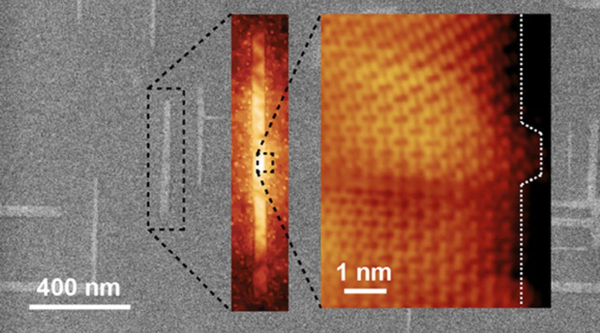
In research published in the journal Nature Communications, the Wisconsin team were able to grow graphene on a conventional germanium semiconductor wafer.
"Graphene nanoribbons that can be grown directly on the surface of a semiconductor like germanium are more compatible with planar processing that's used in the semiconductor industry, and so there would be less of a barrier to integrating these really excellent materials into electronics in the future," said Michael Arnold, an associate professor UW-Madison, in a press release.
Previous bottom-up approaches only worked on metal substrates, and, to date, have not been able to produce nanoribbons with the necessary length to be useful for electronics.
The UW-Madison researchers overcame this limitation by putting a bit of a twist on chemical vapor deposition (CVD)—a technique that has served as a kind of bridge of late between scalability and purity in graphene production. In CVD techniques, the graphene is grown from a vaporous precursor on a metal substrate like copper or nickel in a furnace. What the UW-Madison team did was to start the process with methane, which attaches to the germanium surface and breaks down into various hydrocarbons. These different hydrocarbons then begin to react with each other to form graphene.
The key to the technique is its tenability. The researchers can slow the growth rate of the graphene and thereby both lengthen the nanoribbons and make them narrower by decreasing the amount of methane in the CVD furnace chamber.
"What we've discovered is that when graphene grows on germanium, it naturally forms nanoribbons with these very smooth, armchair edges," Arnold said in the release. "The widths can be very, very narrow and the lengths of the ribbons can be very long, so all the desirable features we want in graphene nanoribbons are happening automatically with this technique."
Dexter Johnson is a contributing editor at IEEE Spectrum, with a focus on nanotechnology.


