Any of us who have done some do-it-yourself home improvements know that there’s a big difference between measuring “by eye” versus taking out a tape measure to get an exact measurement.
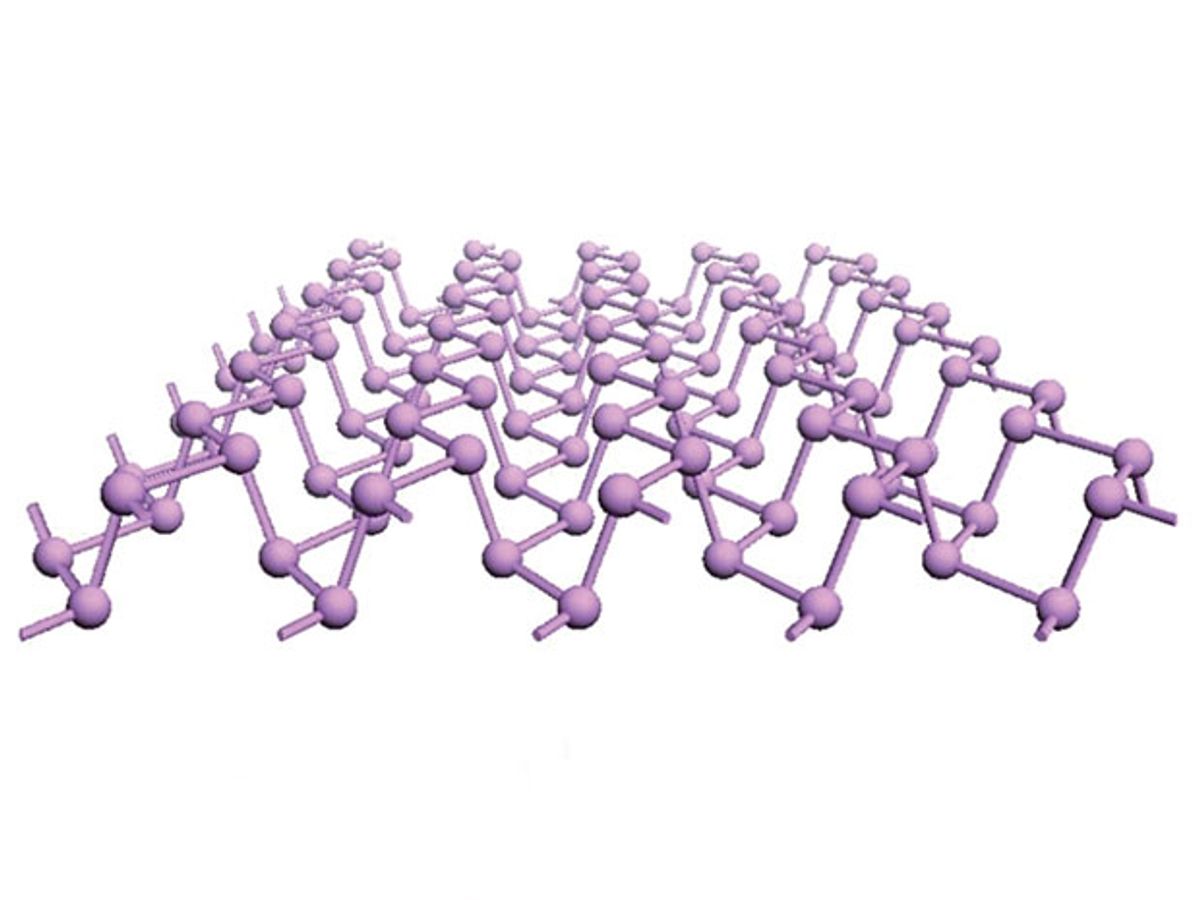
This difference in measurement approaches more or less represents what an international team of researchers from China and the United States have done in measuring the different band gaps that can be created when black phosphorous, also known as phosphorene, is layered.
Previous measurements of the band gaps in layered phosphorene employed fluorescence spectroscopy, which involves using a beam of light to excite electrons in molecules in the test sample, causing them to emit a measurable light. The new, more precise method leveraged in this latest research was optical absorption spectroscopy, in which the absorption of radiation is measured due to its interaction with a sample.
“This is the first measurement based on optical absorption of encapsulated phosphorene,” explained Steven G. Louie, professor of at the University of California Berkeley, in an e-mail interview with IEEE Spectrum. “The optical absorption data are not susceptible to defects and impurities, [unlike] the fluorescence spectroscopy used previously. The encapsulation helps to keep phosphorene from degradation.”
“This work moreover provides the first theoretical understanding how the layers and encapsulation effects tune the band gap, which are shown to be both essential,” added Weng Feng, a professor at UC Berkeley.
In research described in the journal Nature Nanotechnology, the researchers leveraged optical absorption spectroscopy to analyze how the band gap of phosphorene varies significantly with the number of layers, meeting what had been the theoretical predictions. In these measurements, the researchers discovered that the band gaps cover a wide, technologically important spectral range from the visible to the mid-infrared.
Phosphorene’s band gaps have been the main source of excitement within both the electronics and optoelectronics communities because it has a direct bandgap (~0.3 to 2.0 electron Volts (eV)) that covers a regime otherwise unavailable from all other 2-D layered materials. It also bridges the band gap range between those of graphene (zero band gap) and transition metal dichalcogenides (TMDCs, ~1.5 to 2.5eV). Crucially, the band gap of phosphorene corresponds to the optical wavelength in the range of 0.6 to 4.0 microns, covering the visible to infrared range.
In the research, the scientists found that two layers of phosphorene create 1.15 eV, three layers produce 0.83 eV and a band gap of 0.35 eV occurs when the material is in its bulk form.
“The 1.15 eV matches well with the silicon band gap and will be good for many electronic applications. And 0.83 eV is similar to the telecom photon wavelength and will be useful for optoelectronics,” explained Louie. “The 0.35 eV band gap of bulk material may be useful for infrared devices.”
In the next step of the research, the plan is to fabricate optoelectronic devices. But the researchers are under no illusion that this will be a straightforward task.
“The samples are still relatively difficult to deal with, due to small flake sizes and air instability,” explains Feng. “Higher quality bulk samples and more well-defined protection techniques will be helpful. Ultimately, large area growth of few-layer phosphorene will be needed for realistic electronic device applications.”
Dexter Johnson is a contributing editor at IEEE Spectrum, with a focus on nanotechnology.


