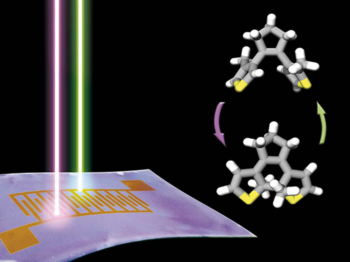
A regular stream of breakthroughs with organic nanomaterials for use in flexible electronics has observers scratching their heads as to why we aren’t seeing more of these technologies in applications such as wearable electronics. The problem has been that although organic nanomaterials have made flexible logic circuits and displays possible, they have pretty much failed to yield flexible, nonvolatile memories with write/erase speeds that would make them practical.
Now a team of researchers hailing from the University of Strasbourg and the Centre National de la Recherche Scientifique (CNRS) in France, along with collaborators from Humboldt University of Berlin and the University of Nova Gorica, in Slovenia, has developed a flexible nonvolatile optical memory thin-film transistor device made from organic nanomaterials that may change the game in wearable electronics.
To date, the major challenge in developing flexible organic memories has been creating a stable system that doesn’t lose data over time (volatility), is flexible, and offers an acceptable number of write/erase cycles (endurance).
The international research team overcame all of those hurdles, but they wanted more. “We wanted every single device to be able to store more than just a single bit (multilevel operation); we achieved 8 bits,” said Emanuele Orgiu, a researcher at CNRS and one of the authors of the paper, in an email interview with IEEE Spectrum.
“In addition, our devices can be made from solutions directly on a plastic substrate, and they feature very fast response times (within nanoseconds)—an intensely sought-after property for organic semiconductors, which usually exhibit very long response times (greater than a millisecond),” added Orgiu.
In a paper published in the journal Nature Nanotechnology, the team explains that it was able to achieve all of this by fabricating the device from molecules known as diarylethenes (DAEs), which can be switched between two states (called either open or closed form). Switching from writing to erasing was as simple as adjusting the wavelength of the light hitting the material (blue light for writing, green for erasing).
“The DAEs used in our work are particularly suited for nonvolatile data storage, since their two forms are stable at ambient conditions,” explained Tim Leydecker, another researcher from CNRS who is a member of the research team. “Plus, they can be switched even when embedded within a semiconducting polymer matrix, making them an ideal candidate for flexible films.”
explains that the molecules’ fast response to a 3-nanosecond laser pulse is relevant to modern electronics. Another benefit of the DAE molecules is that the amount of molecules that are switched in reaction to the light can be precisely controlled, which is a key requirement for multi-level storage that improves the data density.
Paolo Samorì, another team member from CRNS, explained that the molecules’ fast response to a 3-nanosecond laser pulse brings them right in line with modern electronics. Samorì added that another benefit of the DAE molecules is that the number of molecules that are switched in reaction to the light can be precisely controlled—a key requirement for improved data density in multilevel storage.
The devices they have fabricated so far are laboratory prototypes, and thus are relatively large at 1 square millimeter. Needless to say, miniaturization and encapsulation will need to be addressed in order for these memories to become a commercial product. However, the rearchers already have these issues in their sights, and plan to continue testing the performance and stability of the devices after encapsulation.
The team will also be examining fabrication processes compatible with industrial output, such as roll-to-roll manufacturing and inkjet printing.
Stefan Hecht, a team member from Humboldt University of Berlin, added: “Implementation into electronics featuring other organic components (organic light-emitting diodes and organic field-effect transistors) is an important step, as the entire system would benefit from the advantages of organic electronics.”
Dexter Johnson is a contributing editor at IEEE Spectrum, with a focus on nanotechnology.


