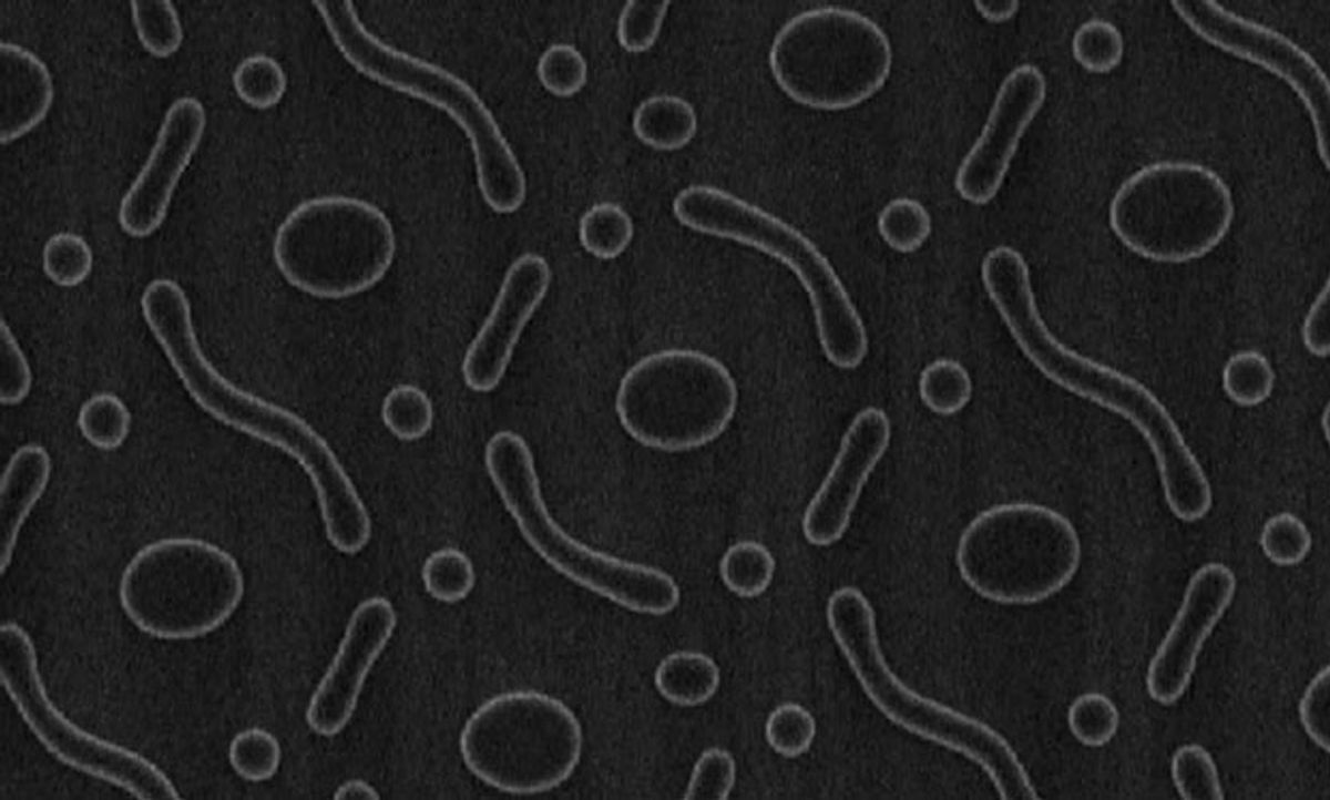
Silicon Valley-based D2S revealed last week that it had solved the last problem in a nascent technique called inverse lithography technology, or ILT. The breakthrough could speed the process of making chips and allow semiconductor fabs to produce more advanced chips without upgrading equipment. The solution, a custom-built computer system, reduces the amount of time needed for a critical step from several weeks to a single day.
In most of the photolithography used to make today’s microchips, light with a wavelength of 193-nanometers is shown through lenses and a patterned photomask, so that the pattern is shrunk down and projected onto the silicon wafer where it defines device and circuit features. (The most modern chip making technology, extreme ultraviolet lithography, works a bit differently. But, only a few chipmakers have these tools.)
However, for about a decade, those features have been much, much smaller than 193 nanometers. That means the one-to-one correlation between the pattern on the mask and the pattern you get on the wafer no longer applies. Without a host of optical tricks, including the addition of odd shapes and severe limits on what kinds of shapes you can use, all you’d get on the wafer is a mess of blurry diffraction patterns.
But what if you could run things backward? Start with the features you want to appear on the wafer and compute which combination of strange shapes on the photomask would produce them. That’s the premise behind inverse lithography technology (ILT). Until now, using ILT across the entire chip layout has been so impractical and time consuming that even the most advanced chipmakers use it only for small areas and fixes.
Two problems kept full-chip ILT out of the mainstream. The first, mask write time, was solved recently with the development of multibeam electron-beam lithography. Electron beams have long been used to write patterns on blank photomasks. However, the technology takes an outsized amount of time if it has to draw curves, and curved shapes are what’s needed to get ILT’s advantages. New systems that can write with thousands of beams of electrons at once have no such limitation, finishing the job in about half a day no matter how many curves are needed.
But even with the ability to draw curves quickly, the sheer computational complexity of inverse lithography made trying to design a mask for an entire chip a multi-month exercise. Conventional ILT approaches tried partitioning the mask design up into computable portions and then stitching the solutions together. But errors abounded at the partition boundaries, and fixing the errors from stitching them together was too time-intensive to be worthwhile.
D2S has now come up with a solution called TrueMask ILT, a GPU-based computer system and the software to run it, which can handle the ILT computation for a full chip in a single day. “Wafer fabs need to deliver wafers in the shortest time possible, which requires ILT process time to be shrunk to a single day in order to be practical,” Leo Pang, chief product officer and executive vice president at D2S, said in a press release. The new system is “the first commercial ILT solution that delivers full-chip ILT within this time constraint.”
The computer’s design allows it to handle the entire chip, because its software combines the system’s many CPUs and GPUs in such a way that they act like a single processor. “We actually created a virtual, gigantic GPU,” explains Pang. The mask no longer needs to be partitioned into several smaller ones for the purpose of computation. “If you can create a gigantic GPU, then the one partition becomes a full chip.”
D2S and memory-chip maker Micron Technology tested the system by creating photomasks for the process layers that require the most stringent tolerances, called contact layers and cut layers. In results presented last week at the SPIE Photomask Technology and EUV Lithography Conference, the new ILT system could produce patterns on the wafer with over 100 percent better tolerance to variations in focus and dosage than today’s technology, called optical proximity correction. “I’ve never seen that in my whole life,” says Pang, who has been working on ILT for more than a decade. “The first time I looked at it, I couldn’t believe it.”
That tolerance—called the process window—translates into some very useful things for chipmakers. “A 100 percent improvement in process window is more than one generation of [photolithography] scanner can achieve,” says Pang. That means a chipmaker could potentially move to a more advanced manufacturing node without purchasing a new photolithography machine.
It could also reduce the expense of a process by removing the need for one or more photomasks. Because 193-nanometer lithography is stretched to its limits, chipmakers have had to use two or even three masks to produce a single layer of the smallest features. ILT might be able to do the same job with one mask, Pang suggests.
For now, the newest generation of lithography machines don’t need ILT, because the light they use, 13.5-nanometer extreme ultraviolet, has a wavelength that’s still smaller than the features it’s being asked to produce. But that could change as the few companies with that technology continue to pursue Moore’s Law.
Samuel K. Moore is the senior editor at IEEE Spectrum in charge of semiconductors coverage. An IEEE member, he has a bachelor's degree in biomedical engineering from Brown University and a master's degree in journalism from New York University.


