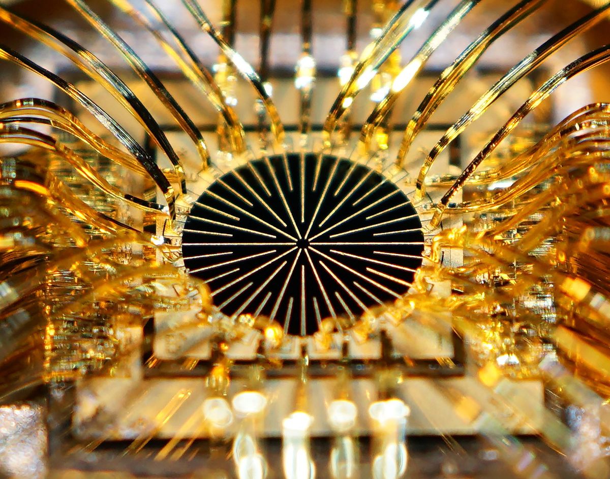
Researchers at North Carolina State University (NCSU), led by Jay Narayan, have developed a new method for converting hexagonal-boron nitride (h-BN) directly into cubic-boron nitride (c-BN) that is faster and less expensive than previous processes and promises to make a material that is more viable for high-power electronics, transistors and solid-state devices.
Boron nitride (BN) comes in four basic forms. Two of these forms of boron nitride, namely hexagonal-boron nitride (h-BN) and cubic-boron nitride (c-BN), represent the two most attractive forms of BN for electronic applications because their structures and properties are quite similar to both graphite and diamonds. Like diamonds, c-BN has very good thermal properties for integrated circuits as well as high-frequency power capabilities that compare favorably with silicon.
The NCSU process can either produce traditional c-BN or a new material they have dubbed Q-BN, with the Q standing for the “quenched” phase of the material, which is created after the BN is heated to a high temperature and cooled rapidly. The development of the Q-BN builds on Narayan’s previous research published last year in the Journal of Applied Physics in which he and his team created a new phase of carbon, dubbed Q-carbon.
“This is a sequel to our Q-carbon discovery and converting Q-carbon into diamond,” said Narayan in a press release. “We have bypassed what were thought to be the limits of boron nitride’s thermodynamics with the help of kinetics and time control to create this new phase of boron nitride.”
In this latest research, published in the journal APL Materials, Narayan and his team fabricated the Q-BN and the c-BN by starting with a layer of thermodynamically stable h-BN that ranged beteween 500-1000 nanometers thick. This h-BN was placed on a substrate where it was hit by high-power laser pulses that heated the h-BN to 2,800 degrees Kelvin or about 2,530 degrees Celsius. The h-BN is then quenched by the substrate that absorbs the heat. The entire process only takes about one-fifth of a microsecond and is conducted entirely at room temperature.
The key to the process is how the researchers manipulate the substrate beneath the h-BN, which determines how quickly the material cools. By controlling this cooling the researchers could determine whether the resulting material would turn out to be traditional c-BN or the new Q-BN.
The advantages over traditional methods of converting h-BN into c-BN are pretty clear. Previous methods for making c-BN involved heating the h-BN to 3,500 degrees Kelvin or 3,225 degrees Celsius and applying 95,000 atmospheres of pressure.
With this faster and cheaper method for making c-BN, it will become easier to exploit c-BN’s advantages over diamonds in electronic applications. For instance, c-BN has a higher band gap than diamonds, which makes it more attractive for high-power devices.
“Since we can create large-area single-crystal films with c-BN and they can be doped with n- and p-type dopants, we can form high-power transistors and switches,” Narayan said in an e-mail interview. “These can replace bulky transformers and create next-generation power grid needed for the super power highway.”
Dexter Johnson is a contributing editor at IEEE Spectrum, with a focus on nanotechnology.