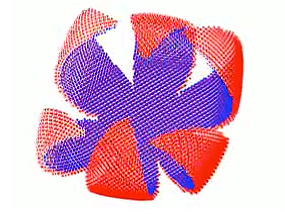
Graphene’s two-dimensional physical attributes have offered some of its most attractive properties. But over the past couple of years, it’s been shown that adding a little wrinkle to the material—effectively making it three-dimensional—offers some new possibilities for the wonder material in wearable electronics and biological or dispensable sensors. However, adding those wrinkles comes at a price: the manipulation is performed under harsh conditions that compromise precision or tunability.
Now, in joint research between Johns Hopkins University and MIT, a team of researchers has developed a benign approach to self-folding graphene that lets it scrunch up into well-defined 3D microstructures.
Prior to this most recent work, graphene has been crumpled into relatively disorganized folded geometries by manipulating the substrate or etching pre-patterned catalysts. Folding has also been achieved with manual probes and by transferring graphene on to thick polymer substrates.
But in research described in the journal Science Advances, David Gracias and Weinan Xu from Johns Hopkins, and Markus Buehler from MIT developed an entirely new approach to making graphene thermally responsive while preserving its intrinsic properties and its ultrathin and flexible nature.
“We have shown that we can fold ultrathin graphene with functionalized thickness as low as 5 nanometers,” said Gracias in an e-mail interview with IEEE Spectrum. “This can be thought of as doing origami with a sheet that is 10,000 times thinner than a sheet of paper.”
Importantly, the process is not only compatible with high throughput lithography and can be implemented on a wafer scale, it is also highly parallel, which is important from a nanomanufacturing and large-scale integration perspective, according to Gracias.
The research team tested the efficacy of their resulting 3D graphene by encapsulating live cells, creating nonlinear resistor and creased transistor devices. These application areas hit on the main hopes for the 3D graphene: wearable electronics and biological sensors.
As Gracias explains, cells and tissues are 3D objects, but many electronic and optical sensors are fabricated on inherently rigid and planar 2D substrates. There is a general belief in the field that ultrathin graphene devices could be used to create more effective sensors for such 3D objects by wrapping sensor elements like a shell or mechanical trap.
“Graphene is attractive for sensing since it can conformally contact these objects while providing enhanced optical signals or enabling electrical measurements in all three dimensions,” adds Gracias.
The wearable electronics aspect of the technology comes about because the precisely engineered creases can introduce a band gap in graphene, which it inherently lacks. The band gap makes it possible to use graphene create transistors in flexible, compact form factors, according to Gracias.
Gracias adds: “We are exploring the creation of graphene shell sensors for bio-sensing and the creation of integrated devices with creased graphene transistor and non-linear resistor modules.”
Dexter Johnson is a contributing editor at IEEE Spectrum, with a focus on nanotechnology.


