A Twist in Graphene Could Make for Tunable Electronic Devices
A single material could be "twisted" into various components of a circuit with distinct electronic properties
Engineering a bandgap into graphene has become almost a rite of passage for research groups who work with the material. While many have accomplished this feat, many more have written off graphene in digital logic applications because of the fact that you have to give it a bandgap.
It turns out that all of that engineering of graphene has revealed another feature: tunable electronic properties. This is accomplished by combining graphene with another material that has a very large bandgap, like boron nitride—so-called heterostructures—or by giving graphene a twist.
Now, an international team of researchers from Columbia University, the National Institute for Materials Science in Tsukuba, Japan, and the Centre National de la Recherche Scientifique (CNRS) in France have overcome some of the limitations that previous attempts to twist graphene have faced.
In research described in the journal Science, the group demonstrated proof of principle for a twisting technique using graphene/boron nitride heterostructures. They showed that their technique can control the rotation of the graphene, and demonstrated how the electrical, optical, and even mechanical properties of the device can be dynamically varied with this technique.
By finding a way to change the angle of the twist of graphene in relation to the boron nitride and even alter that angle after manufacturing, the researchers believe this fresh approach could lead to new kinds of electronic devices.
All of this twisting of graphene with other two-dimensional (2D) materials occurs because there is very low friction between them. Also, there is no strong chemical bonding between the crystal planes, so they slide easily over one another. The researchers realized that a benefit of the low sliding friction is that devices could be intentionally designed to be rotatable, according to Cory Dean, an assistant professor at Columbia and coauthor of the research.
“In our fabrication process, we structure the material to be rotated into the physical shape of a gear,” said Dean. “We then use techniques we previously pioneered to mechanically pick up this nano-sized gear (in this case boron nitride) and place it over top of the active device area (in this case graphene). Once in place, we used an atomic force microscope to push along one tooth of the gear, causing it to rotate.”
What happens to the electronic properties of graphene and boron nitride when they get twisted in relation to each other like this is a bit more complicated.
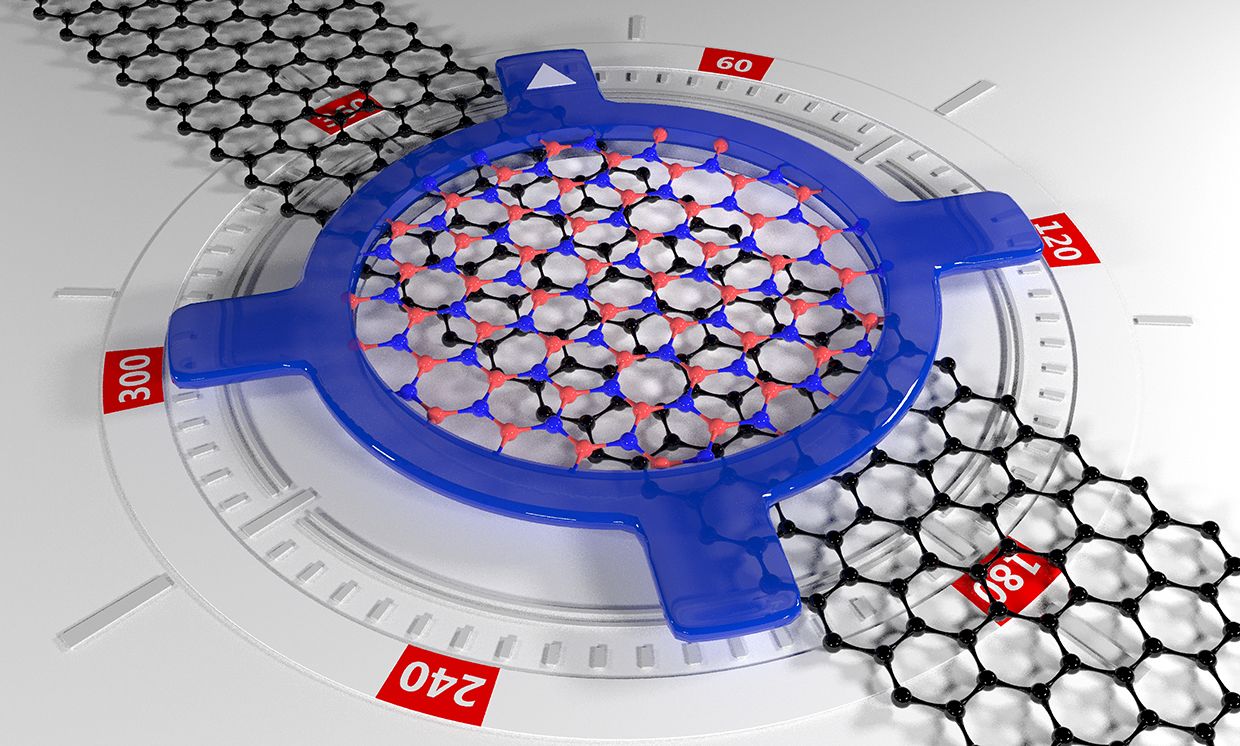
First, boron nitride and graphene have similar honeycomb lattice structures, with only a slight mismatch in their lattices. When they are placed in contact at a zero angle alignment, the small difference in the lattices gives rise to a long wavelength moire pattern, or interference pattern. This moire pattern reflects the length scale over which the two lattices locally transition from being nearly commensurate to being maximally incommensurate.
For electrons moving through the graphene layer, the moire superlattice acts like a periodic scattering potential. The electrons scatter off of this moire superlattice, which modifies their band structure. At a zero angle, this gives rise to a bandgap. When the angle is increased away from zero, the length scale of the moire pattern changes and its influence decreases, so that beyond about 5 degrees, electrons moving through graphene see very little effect of the boron nitride, and intrinsic graphene properties are recovered.
From the standpoint of device engineering, according to Dean, the ability to dynamically change the fundamental electronic response of a material through simple twisting is a new type of control that is difficult to achieve in conventional materials.
“The ability to tune the properties of a layered material by varying the twist angle provides the possibility for a single material platform to perform a variety of functions,” said Dean. “For example, electronic circuits are built from a finite number of components including metallic conductors, insulators, semiconductors, and magnetic materials. This process requires integration of a variety of different materials and can pose a significant engineering challenge. In contrast, a single material that can be locally ‘twisted’ to realize each of these components could enable significant new engineering opportunities.”
A straightforward example of what this tunability could mean comes from the area of switching. Traditional switches typically vary between two well-defined states (on or off, magnetic or not, and so on). This new platform could make it possible to switch between an arbitrary number of complementary states.
So far, the researchers have considered only graphene and boron nitride. However, there is a large class of 2D materials that can be integrated with one another, hosting a variety of intrinsic properties (metallic, insulating, semiconducting, magnetic, superconducting, etc.). Precisely how they couple and how these properties interplay is often dependent on the rotational angle.
Dean added: “The ability to twist these new heterostructures provides a vast new opportunity for realizing tunable interactions between materials with complementary properties.”
Dexter Johnson is a contributing editor at IEEE Spectrum, with a focus on nanotechnology.