New Metal-Air Transistor Replaces Semiconductors
A novel field emission transistor that uses air gaps could breathe life into Moore’s Law
It is widely predicted that the doubling of silicon transistors per unit area every two years will come to an end around 2025 as the technology reaches its physical limits. But researchers at RMIT University in Melbourne, Australia, believe a metal-based field emission air channel transistor (ACT) they have developed could maintain transistor doubling for another two decades.
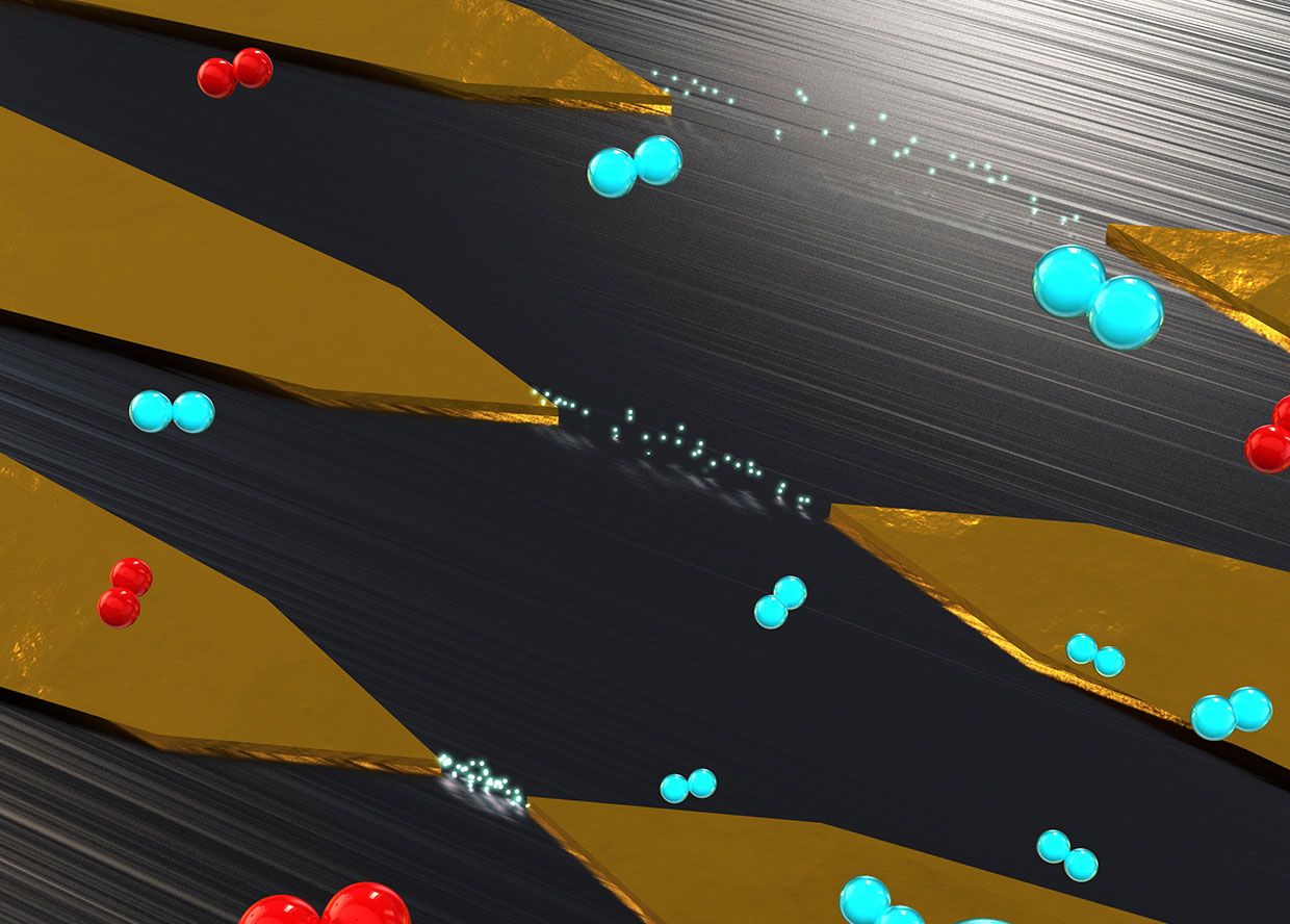
The ACT device eliminates the need for semiconductors. Instead, it uses two in-plane symmetric metal electrodes (source and drain) separated by an air gap of less than 35 nanometers, and a bottom metal gate to tune the field emission. The nanoscale air gap is less than the mean-free path of electrons in air, hence electrons can travel through air under room temperature without scattering.
“Unlike conventional transistors that have to sit in silicon bulk, our device is a bottom-to-top fabrication approach starting with a substrate. This enables us to build fully 3D transistor networks, if we can define optimum air gaps,” says Shruti Nirantar, lead author of a paper on the new transistor published this month in Nano Letters. “This means we can stop pursuing miniaturization, and instead focus on compact 3D architecture, allowing more transistors per unit volume.”
Using metal and air in place of semiconductors for the main components of the transistor has a number of other advantages, says Nirantar, a Ph.D. candidate in RMIT’s Functional Materials and Microsystems Research Group. Fabrication becomes essentially a single-step process of laying down the emitter and collector and defining the air gap. And though standard silicon fabrication processes are employed in producing ACTs, the number of processing steps are far fewer, given that doping, thermal processing, oxidation, and silicide formation are unnecessary. Consequently, production costs should be cut significantly.
In addition, replacing silicon with metal means these ACT devices can be fabricated on any dielectric surface, provided the underlying substrate allows effective modulation of emission current from source to drain with a bottom-gate field.
“Devices can be built on ultrathin glass, plastics, and elastomers,” says Nirantar. “So they could be used in flexible and wearable technologies.”
Replacing the solid-channel transistors in space circuitry is another potential application. Because the electrons flow between the electrodes just as well in a vacuum (think vacuum tube) as in air, radiation will not modulate channel properties, making ACT devices suitable for use in extreme radiation environments and space.
Now that the researchers have proof of concept, the next step is to enhance stability and improve component efficiency by testing different source and drain configurations and using more tolerant materials. In fabricating the prototype ACTs, the researchers used electron-beam lithography and thin-film deposition, while tungsten, gold, and platinum were evaluated as metals of choice.
“We also need to optimize the operating voltage as the electrode metal tips are experiencing localized melting due to concentrated electric fields,” notes Nirantar. “This decreases their sharpness and emission efficiency. So we’re looking at designs that will increase collector efficiency to decrease stress on the emitter.” She believes this can be accomplished over the next two years.
Looking further ahead, she points out that the theoretical speed of an ACT is in the terahertz range, some 10 thousand times as fast as the speed at which current semiconductor devices work. “So further research is needed to find and demonstrate the operational limits,” she adds.
As for commercialization, Nirantar says access to industrial fabrication facilities and support from industry to scale up to 3D networks of the transistors will be necessary. “With such help and sufficient research funding, there is the potential to develop commercial-grade field emission air-channel transistors within the next decade—and that’s a generous timeline. With the right partners, this could happen more quickly.”