There have been increasing signs coming from the research community that carbon nanotubes are beginning to step up to the challenge of offering a real alternative to silicon-based complementary metal-oxide semiconductor (CMOS) transistors.
Now, researchers at IBM Thomas J. Watson Research Center have advanced carbon nanotube-based transistors another step toward meeting the demands of the International Technology Roadmap for Semiconductors (ITRS) for the next decade. The IBM researchers have fabricated a p-channel transistor based on carbon nanotubes that takes up less than half the space of leading silicon technologies while operating at a lower voltage.
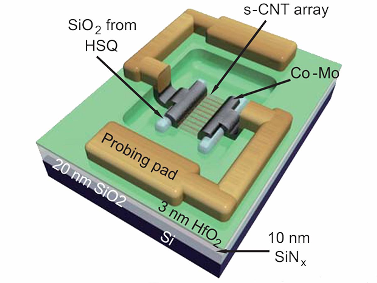
In research described in the journal Science, the IBM scientists used a carbon nanotube p-channel to reduce the transistor footprint; their transistor contains all components to 40 square nanometers, an ITRS roadmap benchmark for ten years out.
One of the keys to being able to reduce the transistor to such a small size is the use of the carbon nanotube as the channel in place of silicon. The nanotube is only 1 nanometer thick. Such thinness offers a significant advantage in electrostatics, so that it’s possible to reduce the device gate length to 10 nanometers without seeing the device performance adversely affected by short-channel effects. An additional benefit of the nanotubes is that the electrons travel much faster, which contributes to a higher level of device performance.
Another key contributor to the small scale of the transistor is the adoption of end-bonded contacts. The metal contacts in transistors have typically been bonded lengthwise along the main body of the transistor’s semiconductor material, resulting in a long contact along the channel. Two years ago, IBM demonstrated that this “end-bond" configuration made it possible to shrink the contact length of the experimental nanotube transistors from 300 nanometers to just 10 nanometers, without any increases in the contact resistance.
To get this to work, the IBM scientists needed a contact metal for the carbon nanotubes that possessed both sufficient thermal stability and reactivity to carbon. It also had to form end-bonded contacts at a temperature low enough to maintain the device geometries. The scientists found that they could adhere the nanotubes to high-work-function cobalt-molybdenum alloy contacts.
The molybdenum maintains the excellent thermal stability of the alloy, while the cobalt serves as a catalyst, reducing the temperature needed to form metal carbide with nanotubes to 650 degrees Celsius.
Since the nanotubes are end-bonded to these contacts, the contacts present a substantial transport barrier for the injection of electrons to the nanotube channel. As a result, the transistors are p-channel only.
“It is challenging to form end-bonded contacts to nanotubes using low-work-function metals for n-channel operation,” explained Qing Cao, Research Staff Member at IBM T.J. Watson Research Center and co-author of the Science paper, in an e-mail interview with IEEE Spectrum. “However, we have already developed some processes to effectively dope the nanotube channel, so that n-channel device operation can be realized even with high-work-function end contacts.”
While there is a work around for achieving n-channel device operation through doping, the device structure does have an out-of-the-box benefit of having a top-gated structure. The top-gated device structure, which is used in today’s silicon transistors, allows easier formation of complex device-to-device interconnects than bottom-gated devices do. This allows for higher device integration density.
In addition to the nanotube channel being end-bonded to cobalt-molybdenum alloy contacts, an ultrathin layer of high-k oxide is sitting on top of the nanotube as the gate dielectric with a metal top gate.
Cao concedes that there are still several manufacturability issues that need to be solved before high-performance nanotube logic transistors become a commercial technology.
“The major challenge at the present stage is device variability,” says Cao. “Ultimately, we want to integrate billions of nanotube transistors into functional circuits. To do this, we need good consistency from one transistor to the next so they can all work together at the same voltage.”
While the purity of semiconducting nanotubes has been significantly improved over the past few years—to the point where IBM has recorded electrically verified purity above 99.999 percent—the process needs to be further standardized and stabilized for reliable large volume production.
“Incorporation of nanotubes into current CMOS processes in a semi-production line has been realized at IBM, but better engineering control is still needed to minimize the amount of impurities in our nanotube source,” adds Cao.
According to Cao, the IBM researchers know that the randomness of fixed charges largely accounts for the variation. But they still don’t fully understand where the charges come from. “Are they mainly from dangling bonds at the oxide surface, from damage to the oxide during the fabrication process, or from residue left by the nanotube solution?”
In terms of engineering, Cao believes that they first need to establish better control over the nanotube source and the deposition process. “The current nanotube solution isn’t really electronic grade, so we may introduce charges on the oxide during the nanotube deposition process,” he says. “Another aspect is to find a better passivation for the nanotube transistors using high-quality, freshly grown dielectrics with no free surface near the nanotube.”
Dexter Johnson is a contributing editor at IEEE Spectrum, with a focus on nanotechnology.


