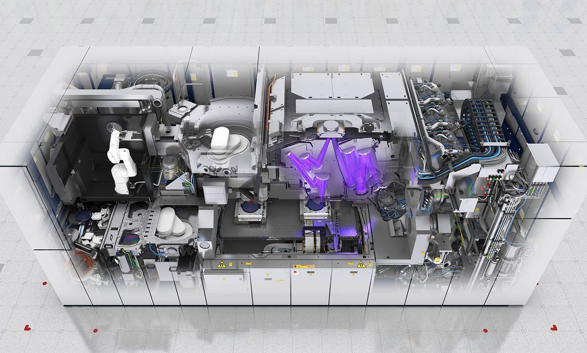
ASML vice president Anthony Yen says that ASML has begun development of the extreme ultraviolet lithography machine his company believes will be needed to continue shrinking the features of silicon chips once today’s systems reach their limits.
The ASML 5000 will rely on a number of evolutionary improvements over the 3400 series, which customers such as Intel, Samsung, and TSMC are using now. The most noticeable will be an increase in the machine’s numerical aperture from today’s 0.33 to 0.55, Yen told engineers at the IEEE International Electron Device Meeting this week in San Francisco. Numerical aperture is a dimensionless quantity related to how tightly light can be focused. A higher numerical aperture means better resolution. Changing the numerical aperture in the EUV machine will require a larger, more perfectly polished set of imaging mirrors.
EUV light is generated by targeting tiny tin droplets with twin pulses from a high-powered carbon dioxide laser. The first pulse reshapes the tin droplet into a hazy pancake shape so that the second pulse, which is more powerful and follows it by just 3 microseconds, can blast the tin into a plasma that shines with 13.5-nanometer light. The light is then collected, focused, and bounced off a patterned mask so that the pattern will be projected onto the silicon wafer.
ASML has increased the number of wafers its machines can process per hour largely by generating more light power. More power means the wafer can be exposed more quickly. At 195 watts they could do 125 wafers per hour; they reached 246 W and 140 wafers per hour early this year. The company has been retrofitting customer machines throughout the year to hit that higher mark.
A next-generation machine will need even more EUV wattage. In the lab, ASML has cracked 410 W, though not yet at a duty cycle good enough for chip production. More powerful lasers will help, and so might increasing the rate at which the tin droplets are zapped. In today’s machines, the tin drops are shot out 50,000 times per second, but Yen showed that the droplet generator could run at 80,000 hertz.
In the meantime, the company is improving the capabilities of its 3400 series. A new version, the 3400C, will be released in the second half of 2019 and surpass 170 wafers per hour. One sore spot in its development had to do with the extremely expensive masks that hold the pattern to be cast onto the silicon. The coverings, called pellicles, which are meant to protect the masks from stray particles, absorbed too much light. ASML says existing pellicles transmit 83 percent of light. This reduces throughput to 116 wafers per hour. The goal is to improve transmission to 90 percent, says Yen. But ASML is also working to keep the inside of the machine even cleaner than it does now, so that customers can feel free to use masks without a pellicle.
Yen says ASML expects to have shipped 18 machines by the end of 2018, and is planning to ship 30 in 2019. However, a fire at a supplier will delay some 2019 deliveries, the company said on Tuesday. ASML lost a prominent customer in August when GlobalFoundries pulled the plug on its 7-nanometer chip development. That move eliminated the need for the two EUV machines the company installed in 2017 and 2018.
Samuel K. Moore is the senior editor at IEEE Spectrum in charge of semiconductors coverage. An IEEE member, he has a bachelor's degree in biomedical engineering from Brown University and a master's degree in journalism from New York University.


