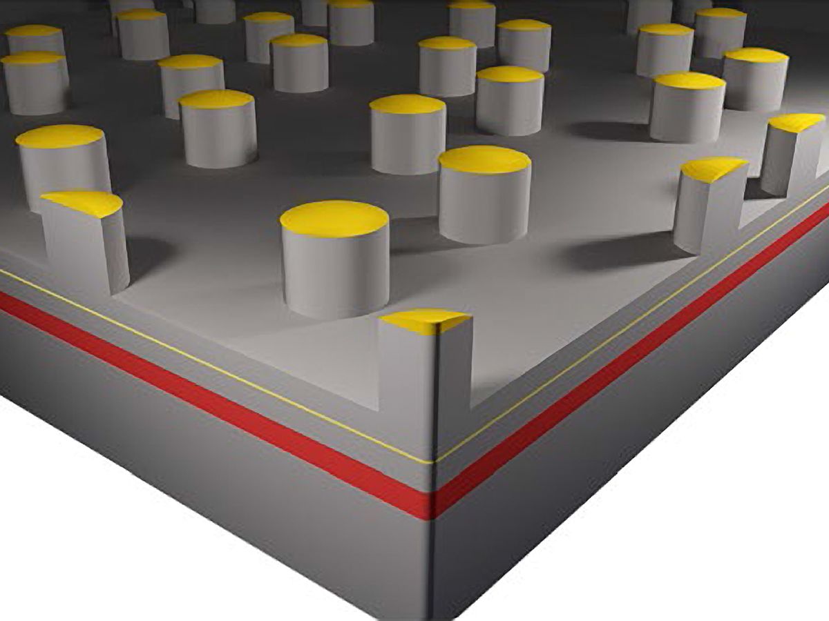
In the last few years, a new form of graphene has garnered increasing interest. Dubbed “artificial graphene,” this latest addition to the 2D landscape is not formed from a single atomic layer of graphite. Instead, it is synthesized from other materials to have the same honeycomb lattice molecular structure as graphene, but modified to have specific electronic properties.
Now a team of researchers from Columbia University and colleagues from Princeton and Purdue Universities along with those from the Instituto Italiano di Tecnologia, in Italy, have taken the next step in artificial graphene by creating for the first time the electronic structure of graphene in a semiconductor device.
The international research team fabricated a solid-state gallium arsenide (GaAs) quantum well, which is a thin layer of material that confines particles such as electrons or holes in the dimension perpendicular to the layer surface. This solid-state semiconductor device marks a big departure from previous uses of artificial graphene that have been restricted to photonic devices.
It has not been easy to wrestle the pure conductor graphene into performing the role of a semiconductor for digital logic applications. Graphene lacks a bandgap, an energy band in which no electron states can exist, which is essential for creating the “on/off” flow of electrons that are needed in digital logic electronics.
While it’s been possible to dope graphene to possess a bandgap like silicon and eke out digital logic functions, it comes at the price of nearly eliminating all the attractive electronic properties of the material. As a result, most have seen that graphene’s electronic properties may prove effective only in photonics and optoelectronic applications.
With this latest development in using artificial graphene in a semiconductor system it becomes possible to envision it being applied to well-developed semiconductor technology.

With the artificial graphene, Lingjie Du, a postdoc researcher in Aron Pinczuk’s research group at Columbia and coauthor of the research, believes that one of the electronic capabilities for this device could be selecting the strength of the spin-orbit coupling in a p-type GaAs quantum well. This could lead to the creation of a topological insulator, which is an insulator on the inside but a conductor on the outside. Such an insulator could in turn enable so-called topological quantum computation, which is a theoretical approach to quantum computing that could be far more robust than current methods. “This capability does not exist in natural graphene or other artificial graphene systems,” said Du.
The semiconductor artificial graphene is realized by the top-down nanofabrication technology, which has the natural advantages of great tunability of electronic states as well as electron device scalability and integration, according to Du.
For example, by integrating two artificial graphene devices with different lattice constants, one can engineer a p-n junction, according to Du, who has also proposed adding strain to honeycomb dot arrays to realize dissipationless current transport, which would address the power issues as devices become smaller in integrated circuits.
While Du acknowledges that GaAs is more expensive than silicon, the nanofabrication technology they have developed could be applied to silicon. However, it might be harder to achieve the level of purity needed by using silicon, resulting in lower signals, Du says.
Dexter Johnson is a contributing editor at IEEE Spectrum, with a focus on nanotechnology.


