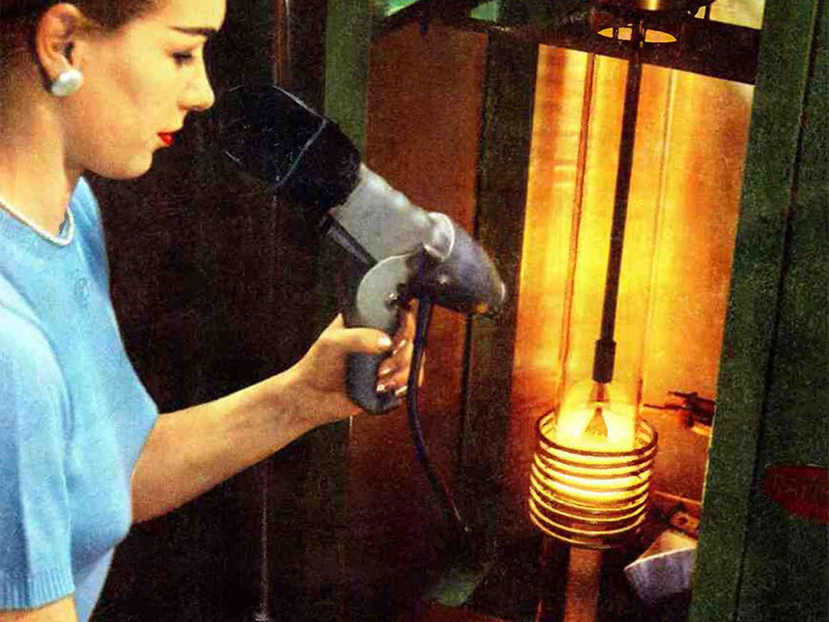
Silicon crystal being grown in 1956 with the Czochralski Method at Raytheon in Waltham, Mass.Photo: Radio and Television News magazine
THE INSTITUTELaptop computers, mobile phones, and a host of other electronic devices wouldn’t exist without semiconductors such as monocrystalline silicon.
Early methods of producing semiconductors were unpredictable and unreliable. There was no way for scientists at the time to prevent the semiconductors from being contaminated by impurities in the air. In 1916, however, Polish chemist Jan Czochralski invented a way to grow single crystals of semiconductors, metals, and synthetic gemstones. The process—known as the Czochralski method—allows scientists to have more control over a semiconductor’s quality and is still used today.
Czochralski discovered the method by accident while working in a laboratory at Allgemeine Elektrizitäts-Gesellschaft (AEG), an electrical-equipment company in Berlin. According to JanCzochralski.com, while investigating the crystallization rates of metal, Czochralski dipped his pen into molten tin instead of an inkwell. That caused a tin filament to form on the pen’s tip. Through further research, he was able to prove that the filament was a single crystal. His discovery prompted him to experiment with the bulk production of single crystals of semiconductors.
The Czochralski process of growing single crystals was dedicated as an IEEE Milestone on 14 November during a ceremony held at the Warsaw University of Technology. The IEEE Poland Section and the IEEE Germany Section sponsored the Milestone. Administered by the IEEE History Center and supported by donors, the Milestone program recognizes outstanding technical developments around the world.

GROWING SILICON
Czochraslski used a silica crucible—a container made of quartz—to grow the crystals. He sat it inside a chamber that was free from oxygen, carbon dioxide, and other potential contaminants. The chamber was surrounded by heaters that converted electric energy into heat. He also used radio waves at a high frequency to melt silicon inside the crucible. When the temperature inside the crucible reached about 1,700 kelvins, it melted the high-purity semiconductor-grade silica.
Once the silicon melted, he placed a small piece of polycrystalline material—a seed crystal—on the end of a 14-centimeter-long, rotating rod. He then slowly lowered the rod into the crucible until the seed crystal dipped just below the surface of the molten silicon. He found that a trace of impurity elements—a dopant—such as boron or phosphorus, could be added to the molten silica in precise amounts to change the silica’s carrier concentration. Depending on what dopants he added, the silica turned into p-type or n-type silicon. They have different electronic properties. When they are put together, they create a diode, which allows for current to flow through the silicon.
Czochraslski simultaneously lifted and rotated the rod that held the seed crystal. During this step, the molten silicon crystallized at the interface of the seed. That formed a new crystal.
The shape of the new crystal, particularly the diameter, can be controlled by adjusting the rod’s heating power, pulling rate, and rotation rate, according to the Encyclopedia of Materials: Science and Technology. That “necking procedure” technique is crucial for limiting the crystal’s structural defects.
Other semiconductors, such as gallium arsenide, also can be grown using the Czochralski method.
The Milestone plaque, mounted at the entrance to the Warsaw University of Technology’s main hall, reads:
In 1916, Jan Czochralski invented a method of crystal growth used to obtain single crystals of semiconductors, metals, salts, and synthetic gemstones during his work at AEG in Berlin, Germany. He developed the process further at the Warsaw University of Technology, Poland. The Czochralski process enabled development of electronic semiconductor devices and modern electronics.
This article was written with assistance from the IEEE History Center, which is funded by donations to the IEEE Foundation’s Realize the Full Potential of IEEE campaign.
Joanna Goodrich is the associate editor of The Institute, covering the work and accomplishments of IEEE members and IEEE and technology-related events. She has a master's degree in health communications from Rutgers University, in New Brunswick, N.J.


