The Conversation (2)

This image of a metalens, taken with a scanning electron microscope, shows the variation in the sizes and layouts of the nanopillars used to manipulate light.
Metalenz
DarkBlue1
Inside today’s computers, phones, and other mobile devices, more and more sensors, processors, and other electronics are fighting for space. Taking up a big part of this valuable real estate are the cameras—just about every gadget needs a camera, or two, three, or more. And the most space-consuming part of the camera is the lens.
The lenses in our mobile devices typically collect and direct incoming light by refraction, using a curve in a transparent material, usually plastic, to bend the rays. So these lenses can’t shrink much more than they already have: To make a camera small, the lens must have a short focal length; but the shorter the focal length, the greater the curvature and therefore the thickness at the center. These highly curved lenses also suffer from all sorts of aberrations, so camera-module manufacturers use multiple lenses to compensate, adding to the camera’s bulk.
With today’s lenses, the size of the camera and image quality are pulling in different directions. The only way to make lenses smaller and better is to replace refractive lenses with a different technology.
That technology exists. It’s the metalens, a device developed at Harvard and commercialized at Metalenz, where I am an applications engineer. We create these devices using traditional semiconductor-processing techniques to build nanostructures onto a flat surface. These nanostructures use a phenomenon called metasurface optics to direct and focus light. These lenses can be extremely thin—a few hundred micrometers thick, about twice the thickness of a human hair. And we can combine the functionality of multiple curved lenses into just one of our devices, further addressing the space crunch and opening up the possibility of new uses for cameras in mobile devices.
Centuries of lens alternatives
Before I tell you how the metalens evolved and how it works, consider a few previous efforts to replace the traditional curved lens.
Conceptually, any device that manipulates light does so by altering its three fundamental properties: phase, polarization, and intensity. The idea that any wave or wave field can be deconstructed down to these properties was proposed by Christiaan Huygens in 1678 and is a guiding principle in all of optics.
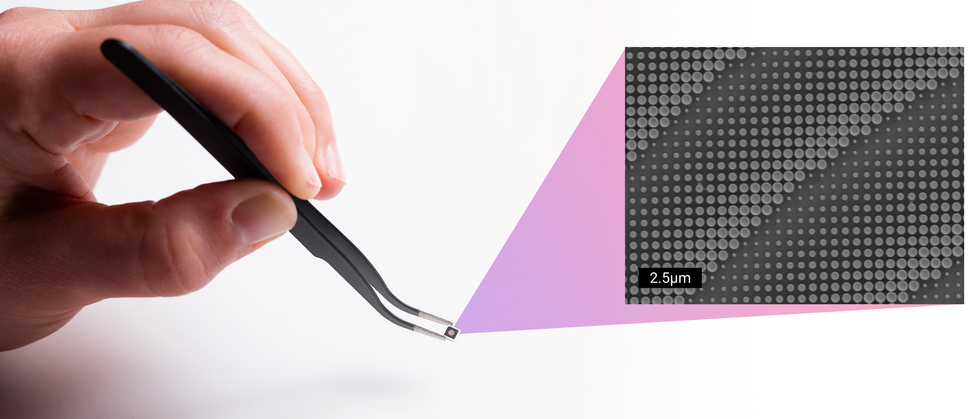 In this single metalens [between tweezers], the pillars are less than 500 nanometers in diameter. The black box at the bottom left of the enlargement represents 2.5 micrometers. Metalenz
In the early 18th century, the world’s most powerful economies placed great importance on the construction of lighthouses with larger and more powerful projection lenses to help protect their shipping interests. However, as these projection lenses grew larger, so did their weight. As a result, the physical size of a lens that could be raised to the top of a lighthouse and structurally supported placed limitations on the power of the beam that could be produced by the lighthouse.
French physicist Augustin-Jean Fresnel realized that if he cut a lens into facets, much of the central thickness of the lens could be removed but still retain the same optical power. The Fresnel lens represented a major improvement in optical technology and is now used in a host of applications, including automotive headlights and brake lights, overhead projectors, and—still—for lighthouse projection lenses. However, the Fresnel lens has limitations. For one, the flat edges of facets become sources of stray light. For another, faceted surfaces are more difficult to manufacture and polish precisely than continuously curved ones are. It’s a no-go for camera lenses, due to the surface accuracy requirements needed to produce good images.
Another approach, now widely used in 3D sensing and machine vision, traces its roots to one of the most famous experiments in modern physics: Thomas Young’s 1802 demonstration of diffraction. This experiment showed that light behaves like a wave, and when the waves meet, they can amplify or cancel one another depending on how far the waves have traveled. The so-called diffractive optical element (DOE) based on this phenomenon uses the wavelike properties of light to create an interference pattern—that is, alternating regions of dark and light, in the form of an array of dots, a grid, or any number of shapes. Today, many mobile devices use DOEs to convert a laser beam into “structured light.” This light pattern is projected, captured by an image sensor, then used by algorithms to create a 3D map of the scene. These tiny DOEs fit nicely into small gadgets, yet they can’t be used to create detailed images. So, again, applications are limited.
Enter the metalens
Enter the metalens. Developed at Harvard by a team led by professor Federico Capasso, then-graduate student Rob Devlin, research associates Reza Khorasaninejad, Wei Ting Chen, and others, metalenses work in a way that’s fundamentally different from any of these other approaches.
A metalens is a flat glass surface with a semiconductor layer on top. Etched in the semiconductor is an array of pillars several hundred nanometers high. These nanopillars can manipulate light waves with a degree of control not possible with traditional refractive lenses.
Imagine a shallow marsh filled with seagrass standing in water. An incoming wave causes the seagrass to sway back and forth, sending pollen flying off into the air. If you think of that incoming wave as light energy, and the nanopillars as the stalks of seagrass, you can picture how the properties of a nanopillar, including its height, thickness, and position next to other nanopillars, might change the distribution of light emerging from the lens.
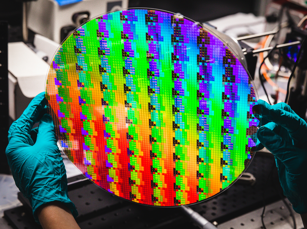 A 12-inch wafer can hold up to 10,000 metalenses, made using a single semiconductor layer.Metalenz
We can use the ability of a metalens to redirect and change light in a number of ways. We can scatter and project light as a field of infrared dots. Invisible to the eye, these dots are used in many smart devices to measure distance, mapping a room or a face. We can sort light by its polarization (more on that in a moment). But probably the best way to explain how we are using these metasurfaces as a lens is by looking at the most familiar lens application—capturing an image.
The process starts by illuminating a scene with a monochromatic light source—a laser. (While using a metalens to capture a full-color image is conceptually possible, that is still a lab experiment and far from commercialization.) The objects in the scene bounce the light all over the place. Some of this light comes back toward the metalens, which is pointed, pillars out, toward the scene. These returning photons hit the tops of the pillars and transfer their energy into vibrations. The vibrations—called plasmons—travel down the pillars. When that energy reaches the bottom of a pillar, it exits as photons, which can be then captured by an image sensor. Those photons don’t need to have the same properties as those that entered the pillars; we can change these properties by the way we design and distribute the pillars.
From concept to commercialization
Researchers around the world have been exploring the concept of metalenses for decades.
In a paper published in 1968 in Soviet Physics Uspekhi, Russian physicist Victor Veselago put the idea of metamaterials on the map, hypothesizing that nothing precluded the existence of a material that exhibits a negative index of refraction. Such a material would interact with light very differently than a normal material would. Where light ordinarily bounces off a material in the form of reflection, it would pass around this type of metamaterial like water going around a boulder in a stream.
It took until 2000 before the theory of metamaterials was implemented in the lab. That year, Richard A. Shelby and colleagues at the University of California, San Diego, demonstrated a negative refractive index metamaterial in the microwave region. They published the discovery in 2001 in Science, causing a stir as people imagined invisibility cloaks. (While intriguing to ponder, creating such a device would require precisely manufacturing and assembling thousands of metasurfaces.)
The first metalens to create high-quality images with visible light came out of Federico Capasso’s lab at Harvard. Demonstrated in 2016, with a description of the research published in Science, the technology immediately drew interest from smartphone manufacturers. Harvard then licensed the foundational intellectual property exclusively to Metalenz, where it has now been commercialized.
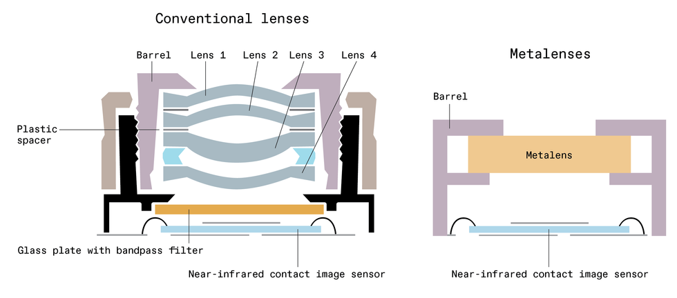 A single metalens [right] can replace a stack of traditional lenses [left], simplifying manufacturing and dramatically reducing the size of a lens package.Metalenz
Since then, researchers at Columbia University, Caltech, and the University of Washington, working with Tsinghua University, in Beijing, have also demonstrated the technology.
Much of the development work Metalenz does involves fine-tuning the way the devices are designed. In order to translate image features like resolution into nanoscale patterns, we developed tools to help calculate the way light waves interact with materials. We then convert those calculations into design files that can be used with standard semiconductor processing equipment.
The first wave of optical metasurfaces to make their way into mobile imaging systems have on the order of 10 million silicon pillars on a single flat surface only a few millimeters square, with each pillar precisely tuned to accept the correct phase of light, a painstaking process even with the help of advanced software. Future generations of the metalens won’t necessarily have more pillars, but they’ll likely have more sophisticated geometries, like sloped edges or asymmetric shapes.
Metalenses migrate to smartphones
Metalenz came out of stealth mode in 2021, announcing that it was getting ready to scale up production of devices. Manufacturing was not as big a challenge as design because the company manufactures metasurfaces using the same materials, lithography, and etching processes that it uses to make integrated circuits.
In fact, metalenses are less demanding to manufacture than even a very simple microchip because they require only a single lithography mask as opposed to the dozens required by a microprocessor. That makes them less prone to defects and less expensive. Moreover, the size of the features on an optical metasurface are measured in hundreds of nanometers, whereas foundries are accustomed to making chips with features that are smaller than 10 nanometers.
And, unlike plastic lenses, metalenses can be made in the same foundries that produce the other chips destined for smartphones. This means they could be directly integrated with the CMOS camera chips on site rather than having to be shipped to another location, which reduces their costs still further.
 A single meta-optic, in combination with an array of laser emitters, can be used to create the type of high-contrast, near-infrared dot or line pattern used in 3D sensing. Metalenz
In 2022, ST Microelectronics announced the integration of Metalenz’s metasurface technology into its FlightSense modules. Previous generations of FlightSense have been used in more than 150 models of smartphones, drones, robots, and vehicles to detect distance. Such products with Metalenz technology inside are already in consumer hands, though ST Microelectronics isn’t releasing specifics.
Indeed, distance sensing is a sweet spot for the current generation of metalens technology, which operates at near-infrared wavelengths. For this application, many consumer electronics companies use a time-of-flight system, which has two optical components: one that transmits light and one that receives it. The transmitting optics are more complicated. These involve multiple lenses that collect light from a laser and transform it to parallel light waves—or, as optical engineers call it, a collimated beam. These also require a diffraction grating that turns the collimated beam into a field of dots. A single metalens can replace all of those transmitting and receiving optics, saving real estate within the device as well as reducing cost.
And a metalens does the field-of-dots job better in difficult lighting conditions because it can illuminate a broader area using less power than a traditional lens, directing more of the light to where you want it.
The future is polarized
Conventional imaging systems, at best, gather information only about the spatial position of objects and their color and brightness.But the light carries another type of information: the orientation of the light waves as they travel through space—that is, the polarization. Future metalens applications will take advantage of the technology’s ability to detect polarized light.
The polarization of light reflecting off an object conveys all sorts of information about that object, including surface texture, type of surface material, and how deeply light penetrates the material before bouncing back to the sensor. Prior to the development of the metalens, a machine vision system would require complex optomechanical subsystems to gather polarization information. These typically rotate a polarizer—structured like a fence to allow only waves oriented at a certain angle to pass through—in front of a sensor. They then monitor how the angle of rotation impacts the amount of light hitting the sensor.
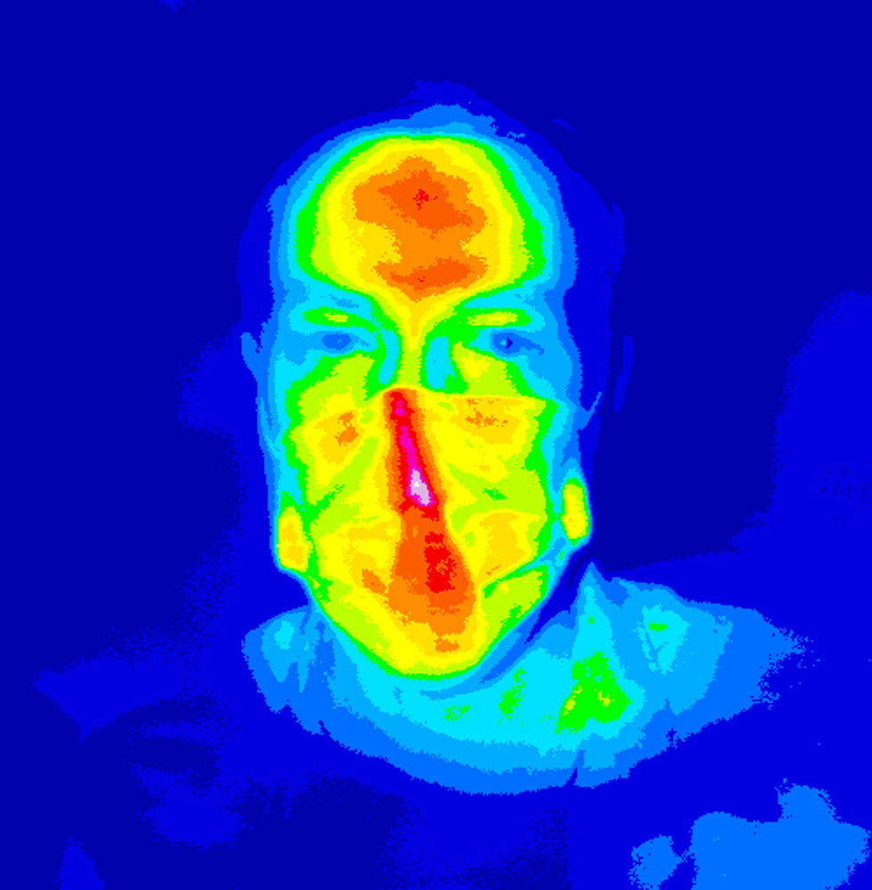 Metasurface optics are capable of capturing polarization information from light, revealing a material’s characteristics and providing depth information.Metalenz
A metalens, by contrast, doesn’t need a fence; all the incoming light comes through. Then it can be redirected to specific regions of the image sensor based on its polarization state, using a single optical element. If, for example, light is polarized along the X axis, the nanostructures of the metasurface will direct the light to one section of the image sensor. However, if it is polarized at 45 degrees to the X axis, the light will be directed to a different section. Then software can reconstruct the image with information about all its polarization states.
Using this technology, we can replace previously large and expensive laboratory equipment with tiny polarization-analysis devices incorporated into smartphones, cars, and even augmented-reality glasses. A smartphone-based polarimeter could let you determine whether a stone in a ring is diamond or glass, whether concrete is cured or needs more time, or whether an expensive hockey stick is worth buying or contains micro cracks. Miniaturized polarimeters could be used to determine whether a bridge’s support beam is at risk of failure, whether a patch on the road is black ice or just wet, or if a patch of green is really a bush or a painted surface being used to hide a tank. These devices could also help enable spoof-proof facial identification, since light reflects off a 2D photo of a person at different angles than a 3D face and from a silicone mask differently than it does from skin. Handheld polarizers could improve remote medical diagnostics—for example, polarization is used in oncology to examine tissue changes.
But like the smartphone itself, it’s hard to predict where metalenses will take us. When Apple introduced the iPhone in 2008, no one could have predicted that it would spawn companies like Uber. In the same way, perhaps the most exciting applications of metalenses are ones we can’t even imagine yet.
From Your Site Articles
- Can Silicon Nanostructures Knock Plastic Lenses Out of Cell Phone Cameras? ›
- Metamaterials - IEEE Spectrum ›
- Tiny Metamaterial Lens Snaps Outsize Images - IEEE Spectrum ›
Related Articles Around the Web