The Conversation (1)

Emily Cooper
Yellow
Photonic integrated circuits, which combine a collection of optoelectronic functions on a single chip, are an increasingly common part of everyday life. They are used in high-speed optical transceivers that link server racks in data centers, including the one used to deliver the IEEE Spectrum website, in lidars to keep self-driving cars on track, and in spectrometers to spot chemicals in the atmosphere, among many other applications. All these systems have grown less expensive and, in some cases have become economically feasible, by making most of the IC with silicon fabrication technologies.
Engineers have been able to integrate nearly every important optical function, including the essentials of modulation and detection, on silicon photonic chips, except for one: light emission. Silicon itself doesn’t do that efficiently, so semiconductors made of so-called III-V materials, named for the place of their constituents on the periodic table, are typically used to make separately packaged components to produce light.
If you can live with an external laser diode in your design, there’s no issue. But several factors have recently been pushing engineers to integrate lasers with silicon photonics. There may be, for example, no space for a separate light source. Tiny devices meant to be implanted in the body to monitor, for example, blood-sugar levels, might face this problem. Or an application’s cost might call for closer integration: When you can fit hundreds or thousands of lasers on a single silicon wafer, you will end up with a lower cost and often higher reliability than when you need to connect separate chips.
There are many ways to achieve this tighter integration of lasers and silicon. Working at Imec, a Belgium-based nanoelectronics R&D center, we are currently pursuing four basic strategies: flip-chip processing, microtransfer printing, wafer bonding, and monolithic integration. What follows is a guide to how these approaches work, their level of scalability and maturity, and their pros and cons.
![]() In flip-chip bonding, laser dies [left] are individually transferred and bonded to a silicon photonics wafer.Emily Cooper
In flip-chip bonding, laser dies [left] are individually transferred and bonded to a silicon photonics wafer.Emily Cooper
Flip-Chip Integration
A straightforward way of directly integrating lasers on silicon wafers is a chip-packaging technology called flip-chip processing, which is very much what it sounds like.
A chip’s electrical connections are on top where the uppermost layer of interconnects terminate on metal pads. Flip-chip technology relies on balls of solder attached to those pads. The chip is then flipped over so the solder lines up with corresponding pads on the chip’s package (or in our case onto another chip). The solder is then melted, bonding the chip to the package.
The concept is similar but more exacting when trying to bond a laser chip to a silicon-photonics chip. Edge-emitting lasers are fully processed on a wafer, diced into individual chips, and tested by the vendor. The individual laser chips are then bonded to the target silicon photonic wafer, using a high-precision version of the flip-chip process, one laser die at a time. The difficult part is ensuring that the output of the laser, which emits at the edge, lines up with the input of the silicon photonics chip. We use a process called butt-coupling, where the laser is placed in a recessed part of the silicon, so it is laterally abutted to the etched facet of a silicon photonics waveguide.
For this to work, the flip-chip process requires submicrometer alignment precision in all three dimensions. Specialized flip-chip bonding tools have been developed over the past several years to do the job, and we and our collaborators and development partners have used them to optimize the assembly processes. Leveraging an advanced pick-and-place tool that uses machine vision to maintain precise alignment, we can place and bond laser devices with precisions better than 500 nanometers in just a few tens of seconds.
In 2021, we also established a wafer-scale silicon-photonics process that improves on this performance. It adds mechanical alignment pedestals and a more precisely etched butt-coupling interface to the silicon chip to achieve vertical alignment of better than a few hundred nanometers. Using these techniques, we assembled certain laser devices on a 300-millimeter silicon photonics wafer. We were delighted to see that as much as 80 percent of the 50 milliwatts of laser light from each device was coupled into the silicon photonics chip to which it was attached. In the worst cases, the coupling was still around 60 percent across the whole wafer. These results rival the kind of coupling efficiencies achieved with active alignment, a more time-consuming process where light from the laser itself is used to steer the alignment process.
A significant advantage of the flip-chip approach is simplicity and flexibility in the kind of chips that get mated. Because they can be produced in existing fabrications lines with limited additional engineering, they can each be sourced from multiple manufacturers. And, with increasing market demand, flip-chip assembly services are being offered by a growing number of vendors. On the other hand, the sequential nature of the process—each laser die needs to be picked up and placed individually—is a significant drawback. It limits the manufacturing throughput and the potential for deep cost reductions in the long run. That’s especially important for cost-sensitive applications, like consumer products, and for systems that require multiple laser devices per chip.
 Laser dies are attached to silicon photonics chips using a high-precision version of the flip-chip method. Optoelectronics
Microtransfer Printing
Microtransfer printing removes some of the alignment difficulties of butt-coupling, while also making the assembly process faster. Just as in flip-chip processing, the light-emitting devices are grown on III-V semiconductor substrates. But there’s a big a difference: The III-V wafers are not diced into individual chips. Instead, the lasers on the wafer are undercut so that they are attached to the source wafer only by small tethers. The devices are then picked up all together with a tool that’s like an ink stamp, breaking the tethers. The stamp then aligns the lasers with waveguide structures on the silicon photonics wafer and bonds them there.
While flip-chip technology uses metallic solder bumps, microtransfer printing uses an adhesive or can even make do with just molecular bonding, which relies on the Van der Waals forces between two flat surfaces, to hold the laser in place. Also, the optical coupling between the light source and the waveguide in the silicon photonics chip happens through a different process. Called evanescent coupling, the process places the laser on top of the silicon waveguide structures and the light “bleeds” into it. Although less power is transferred this way, evanescent coupling demands less precise alignment than does butt-coupling.
Having greater tolerance in alignment enables this technique to transfer thousands of devices at once. So it should, in principle, allow for higher throughput than flip-chip processing and be ideal for applications that ask for the integration of large numbers of III-V components per unit area.
Although transfer printing is an established process for making microLED displays, such as those needed for many augmented reality and virtual reality products, is not yet ready for printing lasers or optical amplifiers. But we’re getting there.
Last year, Imec succeeded in using transfer printing to attach such light sources onto a wafer containing silicon-photonic waveguides, high-speed optical modulators, and photodetectors. We’ve also printed infrared lasers tunable over 45 nm of wavelength and high-pulse energy devices suitable for chip-based spectroscopy systems. These were made only for demonstration purposes, but we see no fundamental reason that this approach can’t achieve good results with high yields. So we expect the technology to be ready for deployment on manufacturing lines within a few years.
![]() In microtransfer printing, laser dies [red rectangles, left] are weakly held in place on their own wafer. A stamp [light grey] picks multiple lasers up at once and places them on the silicon photonics wafer. Emily Cooper
In microtransfer printing, laser dies [red rectangles, left] are weakly held in place on their own wafer. A stamp [light grey] picks multiple lasers up at once and places them on the silicon photonics wafer. Emily Cooper
Die-to-Wafer Bonding
Precisely aligning light-emitting components with their silicon-photonics mates is the critical step in the two technologies we discussed. But one technique, a form of what’s called III-V-to-silicon-wafer bonding, finds a way around that. Instead of transferring already-constructed lasers (or other light-emitting components) to a processed silicon wafer, this scheme bonds blank dies (or even small wafers) of a III-V semiconductor to that silicon wafer. You then build the laser devices you need on top of where the corresponding silicon waveguides already are.
Of the transferred material, we’re only interested in that thin stratum of crystalline III-V material, called the epitaxial layers. So after bonding with the silicon wafer, the rest of the material is removed. Laser diodes can be fabricated in the epitaxial layers aligned to underlying silicon waveguides using standard lithographic and wafer-scale processing. Any unneeded III-V materials is then etched away.
Engineers at Intel developed this approach in the past decade, and the first commercial products built with it, optical transceivers, were launched in 2016. The method allows high throughput integration, because it enables parallel processing of many devices at once. Like transfer printing, it uses evanescent coupling between the III-V and silicon materials, yielding an efficient optical interface.
One drawback of III-V-to-silicon-wafer bonding is that you need substantial investment to establish a manufacturing line that can handle the III-V processing steps using tools meant for fabricating silicon wafers, which are either 200-mm or 300-mm diameter. Such tools are very different from those used in a laser-diode foundry, where the typical wafer diameter is considerably smaller.
![]() In die-to-wafer bonding, blank pieces of III-V semiconductor [pink] are bonded to an already-processed silicon photonics wafer. The III-V material is processed into lasers above the silicon waveguides. The rest of the III-V material is then etched away.Emily Cooper
In die-to-wafer bonding, blank pieces of III-V semiconductor [pink] are bonded to an already-processed silicon photonics wafer. The III-V material is processed into lasers above the silicon waveguides. The rest of the III-V material is then etched away.Emily Cooper
Monolithic Integration
The ideal approach to mating the two different materials involved would be to grow III-V semiconductors directly on silicon, an approach called monolithic integration. This would do away with any need for bonding or alignment, and it would reduce the amount of III-V material that is wasted. But many technological hurdles will have to be overcome for this tactic to be practical. So research toward this goal continues at Imec and elsewhere.
The main aim of that research is to create crystalline III-V materials with a low density of defects. The fundamental problem is that there is quite a mismatch—more than 4 percent—between the lattice spacing of atoms in silicon and that of the atoms in the III-V semiconductors of interest.
Because of this lattice mismatch, every III-V layer grown on the silicon becomes strained. After only a few nanometers of III-V film is added, defects in the crystal emerge, releasing the built-up strain. These “misfit” defects form along lines that penetrate the entire III-V layer. These defects include lines of open crystal bonds and localized crystal distortion, both of which severely degrade the performance of optoelectronic devices.
To prevent these defects from killing the laser, they must be confined to places far from the device. Doing that generally involves laying down a layer of III-V material that is several micrometers thick, forming a hefty buffer between the misfit defects below and a strain-free region above, where the laser devices can be fabricated. Researchers at University of California, Santa Barbara, have reported excellent progress using this approach, demonstrating high-efficiency gallium-arsenide-based quantum-dot lasers with promising reliability lifetimes.
Those experiments have been done only at small scales, however. Extending the technique to the 200- or 300-mm wafers used in industry will be difficult. The addition of thick buffer layers may lead to various mechanical problems, such as cracks developing inside the III-V film or the wafer bowing. In addition, with the active device on top of such a thick buffer layer, it is challenging to couple light to an underlying waveguide in the silicon substrate.
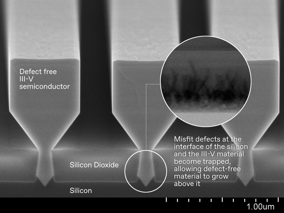
To circumvent these challenges, Imec has introduced a new approach to monolithic integration called nanoridge engineering, or NRE. The technique aims to force defects to form in such a confined space that working devices can be constructed little more than 100 nm above the interface with the underlying silicon.
NRE confines the defects to small regions using a phenomenon called aspect-ratio trapping. It starts by creating narrow and deep trenches inside a layer of silicon dioxide insulator. At the bottom of the trench, where the insulator meets the silicon, a groove cuts into the silicon, giving the void an arrowhead-shaped cross section. A thin layer of III-V crystal is then grown within the trench, and the strain-induced misfit defects are efficiently trapped at the trench sidewalls, preventing these lines of defects from penetrating farther. After the trench is filled, the growth continues to form a larger nanoridge of III-V material above the trench. The material in that nanometer-scale ridge is sufficiently free of defects so that it can be used for laser devices.
Most research on monolithic integration is done at the level of improving individual devices and identifying reasons for their failure. But Imec has already made substantial progress in demonstrating complete wafer-scale integration with this technique, producing high-quality GaAs-based photodiodes in a 300-mm silicon pilot line. The next milestone will be the demonstration of an electrically pumped laser based on a similar design to the photodiodes. Nanoridge engineering is still under development in the lab, but if it works, it will no doubt have a large impact on this industry.
 Nanoridge engineering grows laser-suitable semiconductor in specially-shaped trenches in the silicon. The shape of the trench traps defects [inset] well below the area where the laser is constructed.imec
The Outlook for Lasers on Silicon
In the next few years, each of the approaches discussed here will surely progress further. We expect that they will eventually coexist to serve different application needs and use cases.
The relatively modest setup cost and readiness of flip-chip laser assembly will enable near-term products and is particularly attractive for applications requiring only one or a couple of lasers per photonic IC, such as the optical transceivers used in data centers. In addition, the flexibility inherent in this approach makes it attractive for applications that require nonstandard laser wavelengths or uncommon photonics technology.
For high-volume applications that require multiple lasers or amplifiers per photonic IC, transfer printing and die-to-wafer bonding offer higher manufacturing throughput, smaller coupling losses, and the potential for deeper cost reductions. Because the setup costs here are substantially higher, the applications for which these techniques are suitable will have to have large markets.
Finally, direct III-V epitaxy on silicon, such as the NRE technique, represents the ultimate level of laser integration. But we and other researchers will have to make further progress in material quality and wafer-scale integration to unlock its potential.
The authors wish to thank Katrien Mols.
This article appears in the May 2023 print issue.
From Your Site Articles
- Silicon Photonics Stumbles at the Last Meter ›
- Silicon Photonics - IEEE Spectrum ›
- HPE Invents First Memristor Laser ›
Related Articles Around the Web