
This is part of IEEE Spectrum's special R&D report: They Might Be Giants: Seeds of a Tech Turnaround.
Counting the number of plastic items around you is an exercise only a plastics industry executive could love. The material is ubiquitous--which is just what electronics manufacturers want their products to be when they talk of putting intelligence everywhere.
Quite possibly, organic electronics could make ICs as hard to avoid as plastic, because the devices can be constructed on, and to some degree are made of, plastic. These use semiconducting and sometimes conducting materials that are made of molecules containing carbon, mostly in combination with hydrogen and oxygen. Slower than silicon, but more flexible and potentially much cheaper, organic electronics has already produced circuits with hundreds of transistors printed on plastic, experimental sensors and memories, and displays that bend like paper.
In fact, the current R and D preoccupation in this field is the quest for a cheap, flexible, flat panel display. It is a natural first application. Conventional displays, such as LCDs, are made on glass, which is heavy and brittle. They also rely on manufacturing processes from the microchip industry, and so, the larger they get, the harder they are to make. Given an organic technology capable of creating arbitrarily large displays on lightweight flexible plastic substrates, the uses of flat panel displays could be revolutionized. Researchers envision displays printed onto rolls of plastic, which could be unfurled, processed, and cut up into devices of any size.
To reach this goal, firms are forming collaborations and alliances [see sidebar] that bring together expertise in chemistry and manufacturing techniques from areas other than the microchip industry, as well as more traditional electronics research. R and D in the field is divided into several camps, though there is much overlap. Basically, two types of devices are under development: organic field-effect transistors (OFETs), mainly for the active-matrix backplanes that control display pixels; and organic light-emitting diodes (OLEDs), the pixels themselves. OLEDs, low-power high-brightness devices, are the more mature technology. Products, such as displays for car stereos and cellphones, have been available for a few years, and the first high-volume OLED display shipments began this year.
A second distinction, besides the type of device, is that organic semiconductors come in two flavors. They are either small molecules, such as pentacene, or long chains of molecules--plastic-like polymers--each having different manufacturing requirements. Researchers working in either direction face similar problems, among them device lifetime and manufacturability.
While industry insiders cannot predict whether polymers or small molecules will rule the organic electronics universe in the end, all agree that the deciding factor will be manufacturing costs. Because polymers can be solution-printed like ink, researchers are looking to the printing industry for technology. Small molecules, however, must be evaporated onto a substrate in a vacuum process, akin to those used to make dry-food packaging. Either way circuits will be cheap when future electronics price battles hinge on the technologies that make junk mail and potato chip bags, notes Raj Apte. He heads up organics research at Palo Alto Research Center Inc. (PARC), a recent spinoff from Xerox Corp. [ranked (73) among the Top 100 R and D Spenders in 2001 (PDF)].
Getting it done
Organic electronics R and D requires a different set of lab skills from silicon or IIIV work. Just to do the fundamental research takes expertise in organic chemical synthesis, novel manufacturing techniques, and device physics. Sometimes more than one company is needed to put all that together. In one collaboration, PARC does device physics, Motorola (13) does the manufacturing, and Dow Chemical (65) and the Xerox Research Centre of Canada handle the organic chemistry.
It's rare to find all the needed expertise in one company, but Bell Laboratories (Murray Hill, N.J.) is one of those rarities. It is regarded as the crown jewel of corporate parent Lucent Technologies (17). The lab is historically strong in both chemistry and device physics, and the ease with which cross-fertilization happens there allowed this research to take off.
In the early 1990s, when Bell Labs' organic electronics research was begun by organic chemist Howard E. Katz and electronics engineer Ananth Dodabalapur, the first was a hardcore chemist and the second a self-described "device guy." But both say they have since met in the middle. Dodabalapur, now a professor at the University of Texas at Austin, even supervises chemistry students there. "People at Bell Labs don't draw rigid lines between disciplines," he says. And the space between traditional disciplines has proven fertile ground in the last decade. He and John A. Rogers, who joined the research there in 1997, credit Bell Labs' open structure with the success of the project. The scientists themselves, rather than management, establish projects, and collaborations form spontaneously.
The lab has produced a number of breakthroughs in organic electronics. Among these are useful n-type organic semiconductors, complementary circuits, and plastic-backed active-matrix organic display backplanes (arrays of transistors that drive the pixels of displays). Several firms, including Plastic Logic Ltd. and Royal Philips Electronics (24), have identified plastic backplanes as a major market opportunity and made them a development target. Backplanes for current active-matrix displays use heavy, rigid glass substrates to support their amorphous-silicon thin-film transistors (TFTs). Plastic would be a better substrate, because it is light, bendable, and rugged. But standard amorphous-silicon processing requires temperatures that would melt most plastic.
Conveniently, many organic semiconductors are quite like amorphous silicon with regard to the mobilities of their charge carriers. The speeds with which electrons and holes flit through the semiconductor are the main factor limiting how fast a TFT switches. More importantly, organic materials are flexible, the processes used to deposit them and build them into circuits don't need temperatures above about 100° C, and they lend themselves to large-area manufacturing techniques, some borrowed from the printing industry.
Print, cut, ship
Bell Labs' most frequently demonstrated backplane drives a prototype of what its collaborator E Ink Corp. (Cambridge, Mass.) calls electronic paper--a display that looks like paper and is so flexible it can be bent around a highlighting marker without breaking [see photo, top]. The visible part of the display is a matrix of spheres embedded in a flexible plastic substrate, each sphere encapsulating granules that are sensitive to electric fields. Under the influence of an electric field, the granules move from the bottom of the sphere to the top, making the paper appear white in that spot [see illustration].
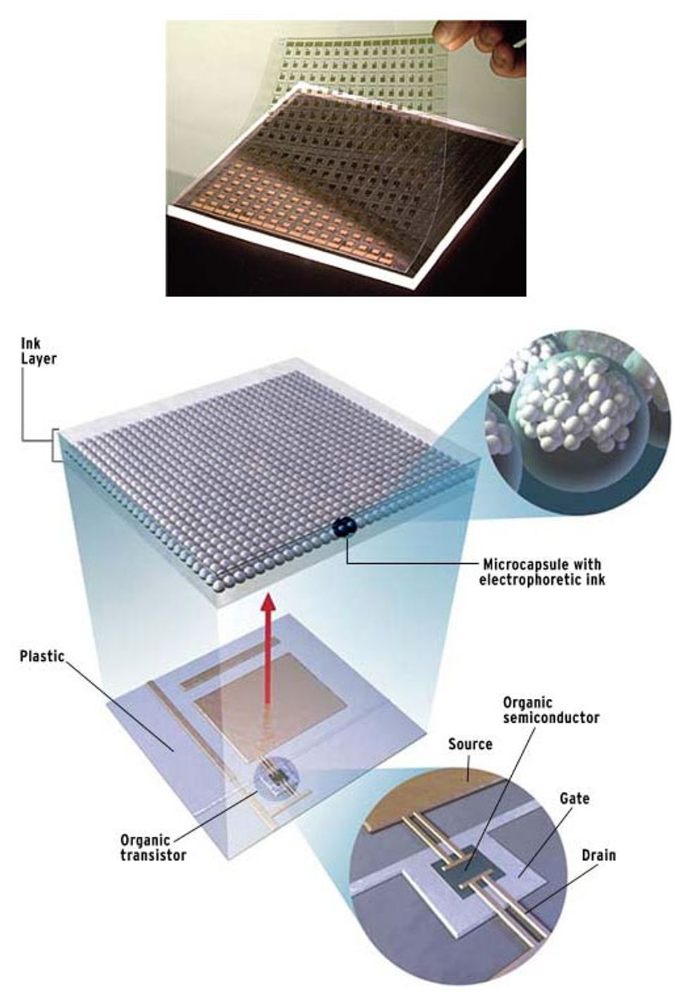
Lightweight and plastic, this device is novel in itself, but without a flexible backplane laminated to it, it's more like wood than paper.
The backplane, which is laminated directly to the microcapsule layer, is composed of OFETs (one per display pixel) and the associated interconnects, all on a sheet of plastic. The OFET itself has a so-called bottom gate construction, with an indium-tin-oxide gate and a polyimide dielectric layer topped with gold source and drain electrodes, and an organic semiconductor such as pentacene in between the source and the drain.
Novel as the semiconducting material may be, the source and drain electrodes were the critical features. The process used to apply them must bec ompatible with plastic and work repeatedly over larger areas than even a 300-mm wafer, but with a resolution of about 10 mm or smaller. Something cheap would be nice, too.
For that the Lucent team uses a so-called soft lithography technique, which Rogers brought with him from Harvard University in 1997. Soft lithography, sometimes called microcontact printing, begins with a slab of rubber that will be used as a stamp. The circuit's features (in this instance, the source and drain electrodes) are etched into the rubber using conventional photolithography techniques. The stamp is then wetted with the organic chemical, hexadecanethiol. Meanwhile, a thin layer of gold has been evaporated onto the circuit substrate [see illustration].
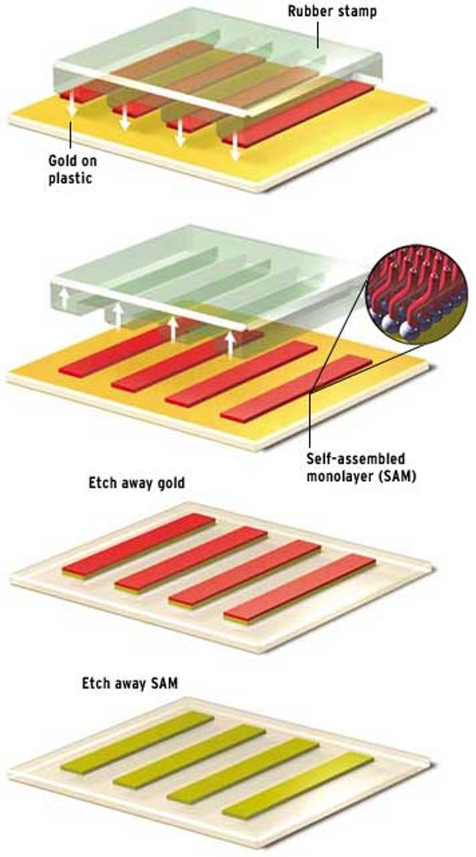
When the stamp is pressed into the substrate, the hexadecanethiol molecules bind to the gold, forming what is called a self-assembled monolayer (SAM). The chemicals in these monolayers automatically attach themselves to gold in a perfectly ordered one-molecule-thick layer. The SAM protects the gold from a chemical etchant applied to dissolve away metal in unprinted areas. The next etchant attacks the SAM, leaving the gold electrodes. Because the stamp was not altered in the process, it can be reused repeatedly.
But microcontact printing isn't the only printing technique being explored for use in organic electronics; laser and inkjet printing techniques are also being adapted. Lucent has recently struck up a partnership with DuPont (54; Wilmington, Del.) to adapt the chemical company's thermal printing technology to organic electronics manufacture [see illustration].
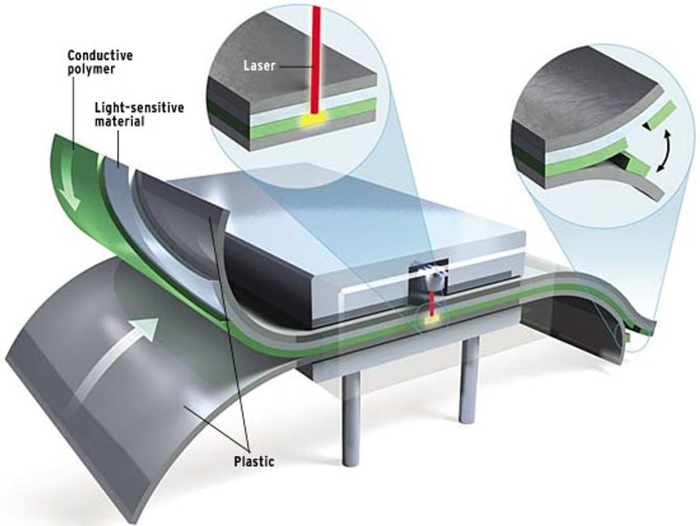
First, a large plastic sheet is coated with an organic compound sensitive to light from a laser used in the printing process. Next comes a layer of conductive polymer that will form the circuit's gate electrodes and interconnects. The coated plastic sheet is then pressed to a second piece of plastic that will act as the circuit substrate, and the two are run through an apparatus that acts like an industrial laser printer.
Wherever the laser strikes, the sensitive compound evaporates, pushing the conductive polymer onto the circuit substrate where it sticks. To build an active-matrix backplane (complete except for the organic semiconductor, which is evaporated on later), the process is repeated using a plastic sheet covered in the gate dielectric and another coated in conductive polymer for the source and drain electrodes. The technique prints all three layers sequentially on a 5-m sheet in about three minutes.
Other firms, including Motorola, Philips Electronics, and Plastic Logic, are interested in inkjet printing techniques not just for the contacts, but for the organic semiconductor itself. While small-molecule organic semiconductors of the kind Lucent uses in its backplane must be evaporated onto the substrate in a vacuum, polymer semiconductors such as polythiophene often can be dissolved in a solution and printed. Although many printing techniques are available, inkjet printing has attracted much attention because it would easily permit changes to the circuit design or even the production of one-off circuits without building new hardware.
"We envision a [manufacturing] platform not too dissimilar from what you'd see in a commercial printing house," says Dan Gamota, department manager and distinguished member of the technical staff at Motorola. The printing industry, he adds, "appears to have the technology to take [organic electronics] to the next level." Because the eye cannot resolve details below 40 mm, commercial printing technology stops there. However, there are ways of going below that limit. And, as in the inorganic world, finer features mean faster circuits.
The first generation of organic fabs, which Gamota expects to be in operation by 2007, will look like printing houses but will borrow technologies from electronics manufacturers, such as in-line testing and machine vision for alignment. The organic fab will be cleaner than a printing house, but nowhere near as strict as the ultra-pure air quality of a semiconductor wafer fab's clean rooms. The price tag, Gamota and others say, will be several orders of magnitude lower than silicon, perhaps costing a few tens of millions of dollars. He sees no reason that, further on, desktop circuit printing machines could not be available.
To be fair, organic materials are not the only hope for flexible circuits. E-ink recently developed a method for creating small-scale polycrystalline silicon backplanes on flexible steel foils, while Rolltronics Corp. (Menlo Park, Calif.) and others are working on cheap ways to make amorphous and polycrystalline silicon circuits on plastic. But proponents believe organic circuits should cost less, be more flexible, and have a greater range of applications than flexible silicon techniques.
Organic pixels in bloom
While organic transistor research focuses on the backplane, organic electronics has already broken onto the market in the display pixels themselves. With OLEDs, the advantage is not just cost but capability. OLEDs have better efficiencies than do incandescent light bulbs, can be printed on plastic substrates, and have none of the viewing angle problems of LCDs. As many as 50 firms have OLED R and D programs, and market analysis firm DisplaySearch (Austin, Texas) predicts rapid market growth from US $84 million today to $1.6 billion in 2007.
Mounting a full frontal attack on LCDs may seem a fool's errand--in early 2002, they were one of the most price-depressed sectors of the electronics business. But industry observers expect that because of the superior image quality, light weight, and low power of OLED displays, the market will bear a slightly higher price for items like OLED-based full-color cellphone displays.
With OLEDs, as with OFETs, the technology divides along the lines between emissive polymers and small molecules. According to Julie Brown, vice president of technology at OLED developer Universal Display Corp (UDC; Ewing, N.J.), small molecules appear to have the upper hand in terms of efficiency, especially for the red-emitting devices crucial to full-color displays. Both emissive polymers and small molecules have the full complement of red, green, and blue emitters, but because of the difficulty of engineering their wider band gap, blue OLEDs lag slightly behind red and green in commercial readiness.
Since OLEDs are already on the market to a limited degree, the challenge now is to cut the cost and extend the lifetimes of devices that come off full-scale manufacturing lines. As in organic transistor technology, polymers can be inked on to the substrate, while small molecules are evaporated through a shadow mask. UDC is developing an improved vapor deposition technique it hopes will meet the flat-panel display industry's requirements for a high-throughput process. [See "Betting on a New Idea," IEEE Spectrum, June 2002, pp. 6364]. But polymer OLED developers such as Cambridge Display Technology are just as confident of solution-based printing techniques. There may be a market for both technologies, but which is going to cost less when scaled to large-area manufacturing? "That's where I think the jury is still out," notes Brown.
Beyond displays
In the early days of organic electronics, attention focused on displays and just a few other applications. Once the technology began to mature, though, the list of potential applications began to grow. Take sensors, for instance.
"It's a very compelling application, because you can connect the organic molecule to a receptor for something you're trying to sense," says Katz. In collaboration with Alan Gelperin, an expert in olfaction at Bell Labs, Katz is designing an array of transistors that can detect and identify chemical vapors in seconds. That's useful for tasks like detecting buried landmines or diagnosing a certain disease by the chemical signature in a patient's breath. In each transistor a positive response is indicated by a decrease in conductance, but since each transistor is made from a different semiconductor compound, it responds more or less strongly to a particular chemical. The array's response pattern uniquely identifies an odor or chemical.
A device of this kind is only possible because Katz's group has designed literally dozens of different semiconductors--more than any other lab. None of the sensor-semiconductors was originally designed for the job, but Katz says his group is zeroing in on ways to engineer them for sensitivity and specificity.
Memory is another new application. Katz is trying to make the all-organic equivalent of the floating-gate transistors used in nonvolatile memory. The bit is stored as charge near the gate dielectric. The charge alters how much current can flow through the transistor.
Intel Corp. (15; Santa Clara, Calif.), too, through a collaboration with Thin Film Electronics ABA (Linkoping, Sweden), is developing a nonvolatile organic memory. In the device, a dipole is built into an organic polymer that is sandwiched between two electrodes. Writing involves polarizing the polymer with an electric field applied between the electrodes; this orients the dipole toward one or the other electrode, signifying a logic 1 or 0. Reading applies an electric field again, and determines the device's state by watching for the flow of current; if the dipole is already lined up with the field, no current flows, but if it is in the other direction, some quantity of charge will flow as the dipole flips over to match the electric field's orientation.
More R and D in the offing
Besides applications development and refined manufacturing techniques, quite a lot of fundamental research remains to be done, including work on organic semiconductors having greater charge-carrier mobilities and operating lifetimes.
The mobility of charge carriers helps define a transistor's switching speed, but is far lower in organic semiconductors than in the crystalline silicon used in ICs. The speed limit is set by the rapidity with which the predominant charge-carriers, holes, can hop from one molecule to another. Granted, organic mobilities have improved in the last decade, but even now, at about 1 cm/V-s, they barely match amorphous silicon. Crystalline silicon's mobility is 500 cm/V-s.
To improve mobility, the molecules must be close together and ordered, but molecular forces and vibrations tend to push them apart. The good news is that researchers now think that transistor action takes place only within the first 5 nm or so from the gate dielectric; so only molecules in that region must be ordered.
Still, at room temperature, there will always be vibrations and unfavorable intermolecular forces to slow things down. "I think it would be difficult to go past 5 [cm/V-s]," says Katz. So do not expect megahertz-speed organic circuits.
"Mobility is the sexy figure of merit," notes PARC's Apte. But he feels it's a bit of a red herring. So-called bias-stress effects, such as hysteresis and drift, are the real enemy. A transistor made from a high-mobility material is no good if its electrical characteristics degrade during operation and it must be turned off for a day just to get them back to normal. "These kinds of effects are not show-stoppers," Apte contends. They were present in early amorphous silicon devices, where engineers were ultimately able to characterize, minimize, and design around them. He believes that the same will be true of organic transistors.
Meanwhile, such effects have hampered reproducing the results of other labs, according to Motorola's Gamota. To tackle the reproducibility problem, he spearheaded the formation of an IEEE standards body to develop uniform testing of organic transistors.
Organic chemistry offers far greater flexibility than silicon or other inorganic chemistry, and the dream is to be able to engineer properties like chemical stability and band gap right into the molecule. But for the moment there is not a solid enough theoretical foundation to do so. Chemists like Katz know how to tweak existing molecules to make them more resistant to oxidation, but any such modification always comes at the cost of another property like mobility.
"It's a shame, because if we had a theoretical understanding, we could really bring to bear all the flexibility in the chemistry," says Rogers. "Right now you only have your intuition to guide you."
To Probe Further
An analysis of the workings of organic light-emitting diodes and other organic circuits is given in "The Dawn of Organic Electronics," by Stephen Forrest, Paul Burrows, and Mark Thompson, IEEE Spectrum, August 2000, pp. 2934.
For Bell Labs' use of rubber stamps to print circuits on plastics, see "Organic Smart Pixels and Complementary Inverter Circuits Formed on Plastic Substrates by Casting and Rubber Stamping," IEEE Electron Device Letters, Vol. 21, no. 3, March 2000, pp. 10003.