Is there a research institute with a more distinguished pedigree in graphene research than the University of Manchester? There certainly haven’t been any that have “gone all in” the way Manchester has with its construction of a $71 million graphene research facility near the campus, which is operated under the auspices of the newly established National Graphene Institute (NGI).
This dedication to graphene makes sense considering the fact that Andre Geim and Konstantin Novoselov were at Manchester when they became the first researchers to synthesize graphene—the advance for which they were awarded the 2010 Nobel Prize in Physics.
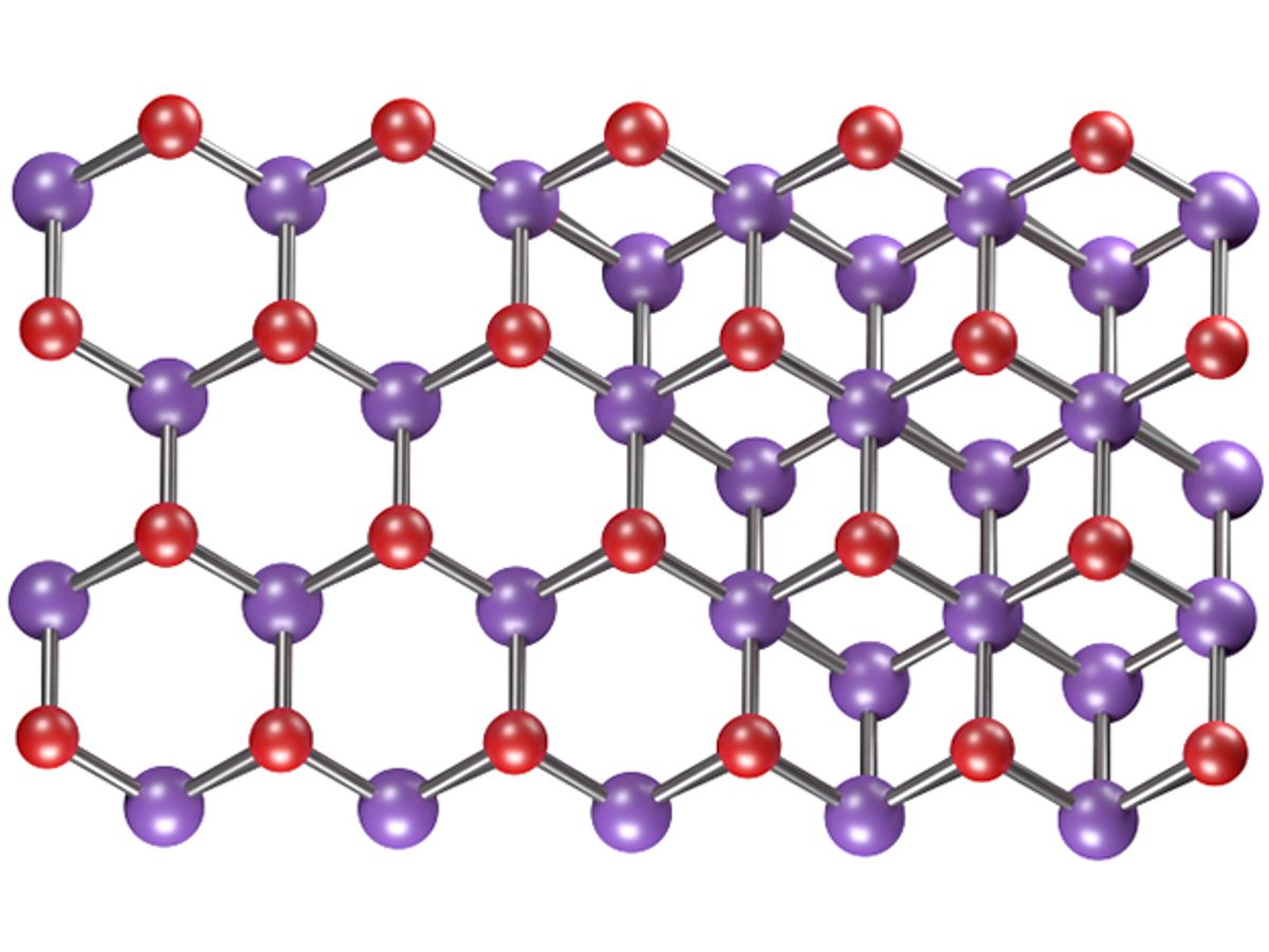
But now it appears that a new material developed at Manchester, based on indium selenide (InSe), has taken some of graphene’s spotlight at Manchester, at least in terms of meeting the demands of future super-fast electronics.
“Ultra-thin InSe seems to offer the golden middle between silicon and graphene,” said Geim in a press release. “Similar to graphene, InSe offers a naturally thin body, allowing scaling to the true nanometer dimensions. Similar to silicon, InSe is a very good semiconductor.”
The semiconductor bit has always been the showstopper for graphene. Because it lacks a natural band gap, that property has to be engineered; but that takes away some of its attractive properties in terms of electron mobility. The form of indium selenide the Manchester researchers have developed has an inherent band gap, and thus requires no gerrymandering that might compromise its high electron mobility.
In research published in the journal Nature Nanotechnology, the Manchester researchers found that the indium selenide had a room-temperature electron mobility of 2,000 square centimeters per Volt-second, which is significantly higher than that of silicon and even higher than few-layer dichalcogenides. Plus, the band gap of the material increases by more than 0.5 electron-volts as its thickness decreases from bulk to bilayers.
These are impressive properties. But all this performance would have been for naught if the Manchester researchers couldn’t find a way to prevent environmental conditions such as oxygen and moisture from ruining the material. The researchers solved this issue by developing a process for synthesizing the material in an argon atmosphere.
Though it’s not certain that graphene has been kicked to the curb in favor of indium selenide, it appears that the last decade spent processing graphene into large sheets may prove beneficial for the manufacturing the new material. Researchers at Manchester believe that it may be possible for indium selenide to be produced at the commercial level in a fairly short amount of time.
Professor Vladimir Falko, coauthor of the paper and director of the National Graphene Institute (NGI) added: “The technology that the NGI has developed for separating atomic layers of materials into high-quality two-dimensional crystals offers great opportunities to create new material systems for optoelectronics applications. We are constantly looking for new layered materials to try.”
Dexter Johnson is a contributing editor at IEEE Spectrum, with a focus on nanotechnology.


