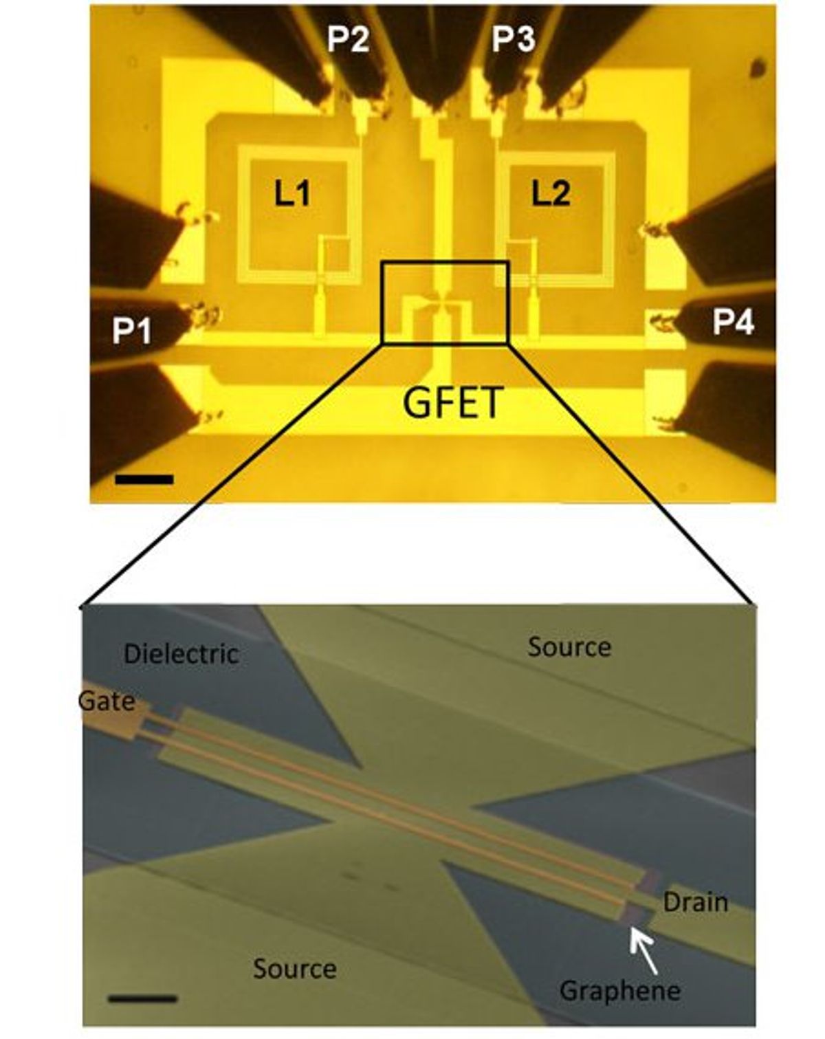
In poker parlance it would seem that IBM has gone “all in” with graphene replacing silicon in the chips of the future.
According to the Spectrum article cited above, it took researchers a year of engineering work to sort how to connect the graphene to the other metallic elements of the circuit and how to perform lithography on it without damaging it.
To overcome the latter challenge the Spectrum article intriguingly says, “One way the team addressed the damage problem was to grow the graphene on a silicon-carbide wafer, then coat it with a common polymer, PMMA, and a resist that was sensitive to jets of electrons used in electron beam lithography.”
I am assuming then that there were other ways tested but this turned out to be the best (I don’t have a Science subscription, so I don’t know if other methods were in fact tried.).
Like anyone who follows to any extent developments in material science around chips I have become somewhat mesmerized at the developments that have been coming fast and furious around graphene.
But meanwhile some interesting developments are occurring with other materials that come in two dimensions like graphene but have a natural band gap. While the molybdenite is not being positioned as a direct competitor with graphene in the post-silicon battlefield, one has to wonder whether there are other minerals out there in addition to molybdenite that could fit the bill and push graphene to the side. Not that there is such a competitor out there mind you, but once upon a time not too long ago carbon nanotubes were the new wonder material that would someday replace silicon. If I were a betting man, I would be looking to hedge my wager somewhat.Dexter Johnson is a contributing editor at IEEE Spectrum, with a focus on nanotechnology.


