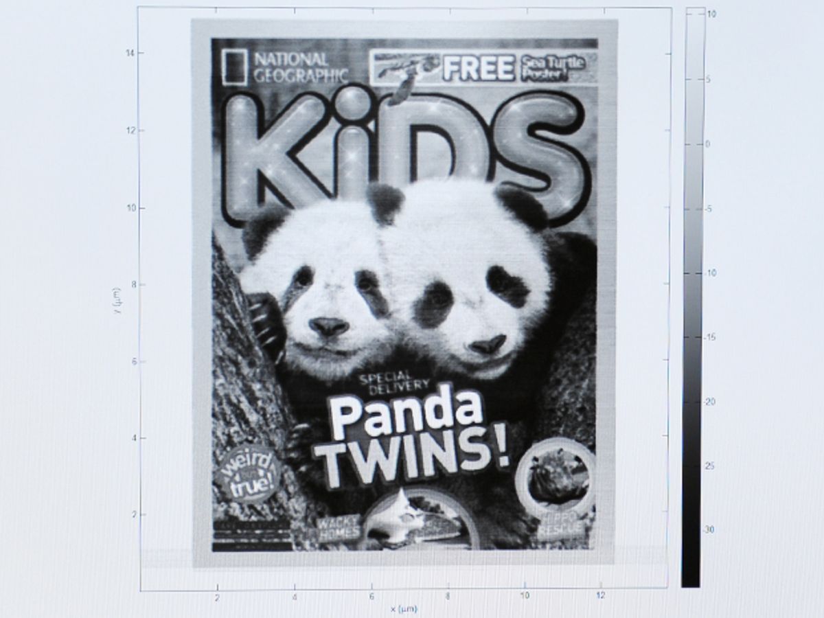
Kids will look through a microscope at the world’s smallest magazine cover at today and tomorrow’s USA Science & Engineering Festival in Washington, DC. When they do, they will see a fuzzy pair of panda twins on the March 2014 cover of National Geographic Kids, the defending champion of Guinness World Records for the smallest magazine cover. This year’s is 11 by 14 micrometers (National Geographic video). Engineers and researchers looking through the microscope, however, might see the cover for what it really is: a demonstration of scanning probe nanolithography’s growing prowess.
Researchers at IBM Research in Zurich, Switzerland, began developing a new method for etching polymers several years ago, as IEEE Spectrum reported in 2010 (“IBM Develops Patterning Technique That Could Replace E-Beam Lithography”). That patterning method used a heated silicon probe to evaporate the material in the substrate, leaving behind the desired pattern in three dimensions. Part of the breakthrough was choosing the right chemistry for the substrate, so that the evaporated chemicals went into a less reactive phase, preventing them from sticking to nearby surfaces.
One of the researchers involved, Urs Duerig, says that was more elegant and cleaner than related lithographic methods, some of which left the excavated debris on nearby surfaces. At first, however, it was too slow for most applications. But by 2011, the team reported a 1000x increase in the speed of their system in the journal Nanotechnology. That speed brings the method on par with existing commercial nanolithography techniques.
The method has another advantage: built-in inspection. After a heated silicon tip evaporates the unwanted material, a second relatively cold tip inspects the results. That’s handier than the industry standard, electron-beam lithography, which requires a separate inspection process. Scanning probe nanolithography may also offer researchers greater control over the depth of the cavities they produce. Duerig claims that they can achieve 1-nm precision. That would enable researchers to create tiny optical cavities, for example, or to create curved structures such as lenses.
IBM licensed the technology to SwissLitho, a spinoff startup founded by researchers from the original team. That team set about creating a machine they could sell to other researchers, and shipped their first one a few weeks ago to a lab at McGill University, which promptly drew a micro-map of Canada.
Maybe for their next publicity stunt they should map the Vatican City.
Lucas Laursen is a journalist covering global development by way of science and technology with special interest in energy and agriculture. He has lived in and reported from the United States, United Kingdom, Switzerland, and Mexico.


