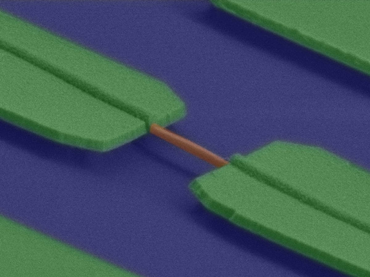
Researchers at IBM Research Zurich and the Norwegian University of Science (NTNU) and Technology have demonstrated for the first time that both efficient light emission and detection functionalities can be achieved in the very same nanowire by applying mechanical strain.
In optical communications, III-V element semiconductor materials are typically used for light emission and silicon or germanium for light detection. By combining both these functions into the same material it may be possible to drastically reduce the complexity of nanophotonic chips.
The researchers, who published their findings in the journal Nature Communications (“Inducing a direct-to-pseudodirect bandgap transition in wurtzite GaAs nanowires with uniaxial stress”), discovered that gallium arsenide can be tuned with a small strain to function efficiently as a single light-emitting diode or a photodetector because of a hexagonal crystal structure, referred to as wurtzite. In wurtzite semiconductors, the atoms are located in very specific positions along the nanowire. That leads to electron and hole wave-functions overlapping strongly but optical transitions between these states being impaired by symmetry. If you change that symmetry with a strain, you can switch between direct or pseudo-direct bandgaps.
"When you pull the nanowire along its length, the nanowire is in a state that we call “direct bandgap” and it can emit light very efficiently; when instead you compress the length of the wire, its electronic properties change and the material stops emitting light,” said IBM scientist Giorgio Signorello in an IBM release. “We call this state “pseudo-direct”: the III-V material behaves similarly to silicon or germanium and becomes a good light detector."
Optical communications are not the only potential applications for this research. "It also gives us a much better understanding, allowing us to design the nanowires with a built-in compressive stress, for example to make them more effective in a solar cell,” said Helge Weman, a professor at NTNU in another release. “This can for instance be used to develop different pressure sensors, or to harvest electric energy when the nanowires are bent.”
Dexter Johnson is a contributing editor at IEEE Spectrum, with a focus on nanotechnology.


