In the first decade of graphene research, the preoccupation was with trying to figure out its properties and what applications it might be suited for. It seems that for the second decade of research—at least at the start—the focus has been on how to better manufacture the wonder material. While the initial research thrust, which expands our understanding of graphene's usefulness, continues, there is an increasing push to find ways to manufacture the material to the specifications required for applications such as electronics.
On the manufacturing front, research seems to be turning to nature for direction. We’ve seen it recently in efforts using “survival of the fittest” crystal growth schemes. And in the latest bit of research out of the National University of Singapore (NUS), researchers who mimicked the way beetles and tree frogs keep their feet attached to submerged leaves achieved, for the first time, both the hoped-for growth and transferability of high-quality graphene onto silicon.
The NUS research, which was published in the journal Nature (“Face-to-face transfer of wafer-scale graphene film”), addressed the fundamental problems of growing large films of graphene through chemical vapor deposition (CVD) on copper and then removing them. While CVD processes yield a high-quality graphene (though, to date, not on the level of that produced by mechanical cleavage of graphite—the so-called “Scotch-tape” method) and promises roll-to-roll production of the material, taking the graphene films off the copper is exceedingly difficult because of the impurities of the copper.
The NUS researchers have dubbed their technique “face-to-face” transfer because the graphene is grown on the copper while the copper sits on top of a silicon substrate. Instead of tearing away the graphene, the copper is etched away while the graphene is lashed to the silicon by bubbles that form capillary bridges; this is the same phenomenon that lets the feet of beetles and frogs adhere to submerged leaves. The trick to achieving the capillary bridges—ensuring that the two layers do not delaminate during the etching away of the copper—was injecting gases into the wafer.
“The direct growth of graphene film on silicon wafer is useful for enabling multiple optoelectronic applications, but current research efforts remain grounded at the proof-of-concept stage,” says Professor Loh Kian Ping, who heads the Department of Chemistry at the NUS Faculty of Science, in a press release. “A transfer method serving this market segment is definitely needed, and has been neglected in the hype for flexible devices.”
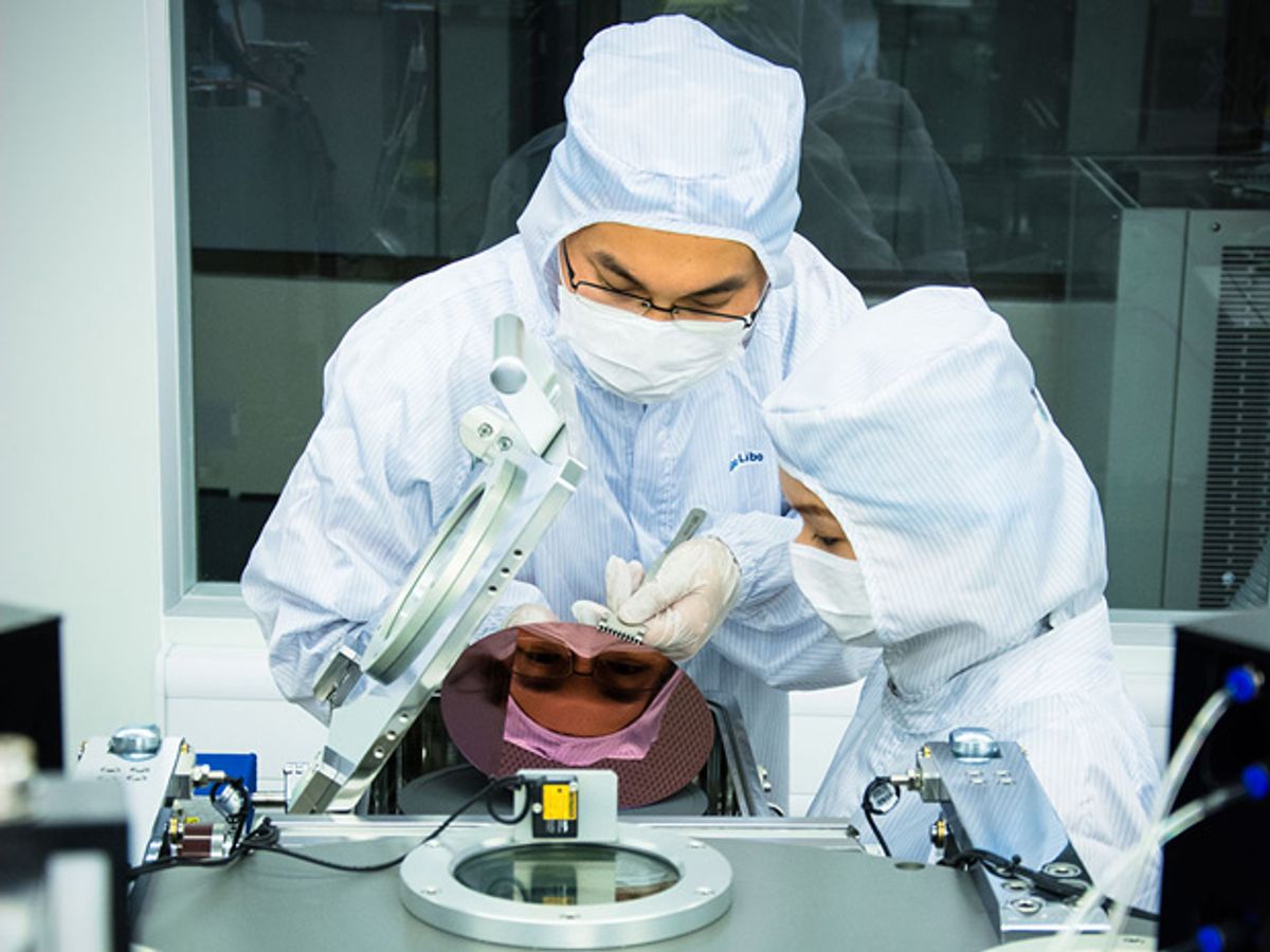
The NUS team believes the “face-to-face” transfer method would be useful in batch-processed semiconductor production lines.
Photo: National University of Singapore
Dexter Johnson is a contributing editor at IEEE Spectrum, with a focus on nanotechnology.


