As the demand for data storage explodes, semiconductor manufacturers are racing to increase the density of memory chips while reducing the cost per bit. Intel and SK Hynix presented two important advances hinting at cheaper solid-state memory drives with higher capacity at the 70th IEEE International Solid State Circuits Conference (ISSCC), held in San Francisco in late February.
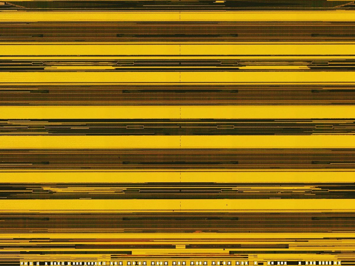
Intel presented the first three-dimensional NAND flash-memory chip that stores five bits of data in each NAND flash cell. That’s one bit more than the 4-bit-per-cell drives that are commercially available today. The 192-layer chip boasts the highest data density yet at 23 gigabits per square millimeter and can store up to 1.67 terabits of data total.
Korea’s SK Hynix, meanwhile, has crossed the 300-layer threshold with a 1-Tb NAND flash-memory chip. The chip stores 3 bits per cell (called triple layer cell, or TLC) and has the highest write speed reported yet, at 194 megabytes per second. Samsung previously had the best write throughput at 184 MB/s for a 3 bits per cell NAND flash memory that they presented at the 2021 ISSCC.
“I believe we presented the best density and write throughput for a TLC product,” says Seungpil Lee, the vice president of SK Hynix’s NAND design department.
NAND flash-memory manufacturers made the jump from 2D to 3D in the past decade to get beyond the constraints of feature-size reduction. Since then, they have regularly upped storage density by increasing the number of layers of flash cells in a chip, or by increasing the number of bits stored in each cell. Hynix and Intel took those two contrasting paths—Hynix by stacking more layers, Intel by densifying bits.
TLC is the most widely used flash today, even though 4-bits-per-cell chips are on the market. Lee says that Hynix is looking into increasing both layer number and the number of bits per cell. More layers give higher performance and bit density in TLC, he says. Increasing the number of bits per cell, on the other hand, can give bigger and cheaper memory, but it affects performance by compromising read and write speeds.
At the 2021 IEEE International Electron Devices Meeting, Samsung’s chairman Kinam Kim predicted that 1,000-layer flash could be possible by 2030. That is vastly challenging from a manufacturing standpoint. Flash cells are made by etching deep, narrow holes through alternating layers of conductor and insulator, and then filling the holes with dielectric and other materials. Etching and filling deep-enough holes reliably and quickly through an increasing number of layers is a key limit to the technology.
Beyond the fabrication issue, when the number of stack layers passes 300, it becomes increasingly challenging to improve NAND-memory performance, Lee says. That’s because each layer in the stack has to be made thinner, which increases resistance. This introduces errors and reduces read and write speeds. Hynix used five different techniques to overcome those challenges and achieve high write throughput with 300 layers.
Intel says it was able to develop its new high-density 5-bit-per-cell chip because of the floating gate NAND cell technology it has chosen to stick with. That design stores bits in a conducting layer. Most other manufacturers have chosen the other main flash-cell technology, charge-trap flash, in which charges are stored in a dielectric layer, because it reduces manufacturing cost.
Going to 5 bits per cell brings concerns of lower endurance and speeds. Intel implemented special fast-read algorithms to overcome that. Plus, the company says that the new chip can also be operated in either a 3-bit-per-cell or 4-bit-per-cell mode.
Micron Technology was the first to cross the 200-layer mark, last year, and is now taking orders for its 232-layer NAND flash-memory technology which has a bit-storage density of 14.6 gigabits per square millimeter, double that of competitors on the market. Not to be left behind, SK Hynix says it will begin volume manufacturing of its 238-layer TLC NAND chips this year.
Prachi Patel is a freelance journalist based in Pittsburgh. She writes about energy, biotechnology, materials science, nanotechnology, and computing.


